EVALSF3-ICE3B2065P Infineon Technologies, EVALSF3-ICE3B2065P Datasheet - Page 10
EVALSF3-ICE3B2065P
Manufacturer Part Number
EVALSF3-ICE3B2065P
Description
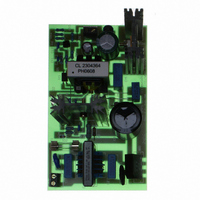
BOARD DEMO ICE3B2065P 40W SMPS
Manufacturer
Infineon Technologies
Series
CoolSET®F3r
Datasheet
1.EVALSF3-ICE3B2065P.pdf
(20 pages)
Specifications of EVALSF3-ICE3B2065P
Main Purpose
AC/DC, Primary Side
Outputs And Type
1, Isolated
Power - Output
40W
Voltage - Output
18V
Current - Output
2.22A
Voltage - Input
85 ~ 265VAC
Regulator Topology
Flyback
Frequency - Switching
67kHz
Board Type
Fully Populated
Utilized Ic / Part
ICE3B2065
Lead Free Status / RoHS Status
Lead free / RoHS Compliant
Other names
EVALSF3-ICE3B2065PIN


6
6.1
The AC line input side comprises the input fuse F1 as over-current protection. The choke EMI1, X2-
capacitors C1, C2 and Y2-capacitor CY1 act as radio interference suppressors. After the bridge rectifier BR1
and the input capacitor C3, there is a voltage of 90 to 380 VDC depending on input voltage. The varistor
VAR1 after fuse can absorb the input surge transient voltage and the thermistor RT1 can limit the input
inrush current during the first plug in of the AC input line.
6.2
The PWM pulse is generated by the 6-pin CoolSET™F3 ICE3B2065P. ICE3B2065P is an integrated power
IC which includes the current-mode PWM controller and a CoolMOS
control IC and CoolMOS
monolithic approaches is necessary.
6.3
Since there is a built-in startup cell in the ICE3B2065P, there is no need for external start up resistor. The
startup cell is connecting the drain pin of the IC. Once the voltage is built up at the Drain pin of the
ICE3B2065P, the startup cell will charge up the Vcc capacitor C6 and C7. When the Vcc voltage exceeds
the UVLO at 15V, the IC starts up. Then the Vcc voltage is bootstrapped by the auxiliary winding to sustain
the operation.
6.4
The Soft-Start function is realized by an internal resistor and the adjustable external capacitor C5.
6.5
During operation, the Vcc pin is supplied via a separate transformer winding with associated rectification D2
and buffering C6, C7. Resistor R2 is used for current limiting. In order not to exceed the maximum voltage at
Vcc pin an external zener diode Z1 and resistor R2a is added to limit this voltage. C9 can reduce the
switching speed and reduce the switching noise.
6.6
The circuit R1, C4 and D1 clamp the DRAIN voltage spike caused by transformer leakage inductance to a
safe value below the drain source break down voltage V
6.7
The primary current is sensed by the external shunt resistor R3, R4. The sense voltage is fed into
ICE3B2065P and a cycle by cycle current limiting is achieved. Primary current is being converted to a
corresponding voltage level at CS ( I
edge spikes from distorting the current limiting.
1
Application Note
V
DSBR
= 650V @ Tj = 110°C
Circuit Description
Line Input
Power Control and Power Stage
Startup
Soft start
Operation mode
Clamping Network
Primary Current Sense
TM
are fabricated by different optimized chip technologies and no compromise
sense
) pin. A 220ns leading edge blanking is provided to avoid leading
40W 18V Demoboard using ICE3B2065P on board
10
DSBR
= 650V
1
maximum.
TM
with 650V breakdown voltage. The
2006-07-18
Related parts for EVALSF3-ICE3B2065P
Image
Part Number
Description
Manufacturer
Datasheet
Request
R

Part Number:
Description:
BOARD DEMO ICE3DS01G 60W SO-8
Manufacturer:
Infineon Technologies
Datasheet:

Part Number:
Description:
BOARD DEMO ICE3A5565P 100W SMPS
Manufacturer:
Infineon Technologies
Datasheet:

Part Number:
Description:
BOARD DEMO ICE3B0565 15W SMPS
Manufacturer:
Infineon Technologies
Datasheet:

Part Number:
Description:
BOARD DEMO ICE3B2565 30.4W SMPS
Manufacturer:
Infineon Technologies
Datasheet:

Part Number:
Description:
BOARD DEMO ICE3DS01 60W 8-DIP
Manufacturer:
Infineon Technologies
Datasheet:

Part Number:
Description:
BOARD DEMO ICE3B1565 20W SMPS
Manufacturer:
Infineon Technologies
Datasheet:

Part Number:
Description:
Manufacturer:
Infineon Technologies AG
Datasheet:
Part Number:
Description:
Manufacturer:
Infineon Technologies AG
Datasheet:
Part Number:
Description:
Manufacturer:
Infineon Technologies AG
Datasheet:
Part Number:
Description:
Manufacturer:
Infineon Technologies AG
Datasheet:
Part Number:
Description:
Manufacturer:
Infineon Technologies AG
Datasheet:
Part Number:
Description:
Manufacturer:
Infineon Technologies AG
Datasheet:
Part Number:
Description:
Manufacturer:
Infineon Technologies AG
Datasheet:
Part Number:
Description:
16-bit microcontroller with 2x2 KByte RAM
Manufacturer:
Infineon Technologies AG
Datasheet:
Part Number:
Description:
NPN silicon RF transistor
Manufacturer:
Infineon Technologies AG
Datasheet: