AT91SAM9M10-G45-EK Atmel, AT91SAM9M10-G45-EK Datasheet - Page 17
AT91SAM9M10-G45-EK
Manufacturer Part Number
AT91SAM9M10-G45-EK
Description
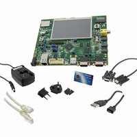
KIT EVAL FOR AT91SAMG45/9M10
Manufacturer
Atmel
Series
AT91SAM Smart ARMr
Type
MCUr
Specifications of AT91SAM9M10-G45-EK
Contents
Board, Cables, Power Supply
Processor To Be Evaluated
AT91SAM9M10
Processor Series
AT91SAM9
Data Bus Width
32 bit
Interface Type
RS-232, Ethernet, USB, JTAG
Operating Supply Voltage
5 V
Silicon Manufacturer
Atmel
Core Architecture
AVR
Kit Contents
Board
Features
Two High Speed USB Hosts, LCD TFT Display
Svhc
No SVHC (15-Dec-2010)
Mcu Supported Families
AT91SAM9M10,
Rohs Compliant
Yes
For Use With/related Products
AT91SAM9M10
Lead Free Status / RoHS Status
Lead free / RoHS Compliant
Available stocks
Company
Part Number
Manufacturer
Quantity
Price
Company:

Part Number:
AT91SAM9M10-G45-EK
Manufacturer:
INFINEON
Quantity:
10 000
Company:
Part Number:
AT91SAM9M10-G45-EK
Manufacturer:
Atmel
Quantity:
135


6.2.2
Table 6-1.
6.2.3
6.3
6.3.1
6.3.2
6355B–ATARM–21-Jun-10
seen at 0x100000 through AHB
SRAM A ITCM size (KBytes)
I/O Drive Selection and Delay Control
TCM Interface
Internal ROM
I/O Drive Selection
Delay Control
ITCM and DTCM Memory Configuration
32
0
0
On the processor side, this Internal SRAM can be allocated to two areas.
Within the 64 Kbyte SRAM size available, the amount of memory assigned to each block is soft-
ware programmable according to
The AT91SAM9M10 embeds an Internal ROM, which contains the boot ROM and SAM-BA
program.
At any time, the ROM is mapped at address 0x0040 0000. It is also accessible at address 0x0
(BMS =1) after the reset and before the Remap Command.
The aim of this control is to adapt the signal drive to the frequency. Two bits allow the user to
select High or Low drive for memories data/address/ctrl signals.
To avoid the simultaneous switching of all the I/Os, a delay can be inserted on the different EBI,
DDR2 and PIO lines.
• Internal SRAM A is the ARM926EJ-S Instruction TCM. The user can map this SRAM block
• Internal SRAM B is the ARM926EJ-S Data TCM. The user can map this SRAM block
• Internal SRAM C is only accessible by all the AHB Masters. After reset and until the Remap
• Setting the bit [17], EBI_DRIVE, in the EBI_CSA register of the matrix allows to control the
• Setting the bit [18], DDR_DRIVE, in the EBI_CSA register of the matrix allows to control the
anywhere in the ARM926 instruction memory space using CP15 instructions and the TCR
configuration register located in the Chip Configuration User Interface. This SRAM block is
also accessible by the ARM926 Masters and by the AHB Masters through the AHB bus
anywhere in the ARM926 data memory space using CP15 instructions. This SRAM block is
also accessible by the ARM926 Data Master and by the AHB Masters through the AHB bus.
Command is performed, this SRAM block is accessible through the AHB bus at address
0x0030 0000 by all the AHB Masters. After Remap, this SRAM block also becomes
accessible through the AHB bus at address 0x0 by the ARM926 Instruction and the ARM926
Data Masters.
drive of the EBI.
drive of the DDR.
seen at 0x200000 through AHB
SRAM B DTCM size (KBytes)
64
32
0
Table
6-1.
seen at 0x300000 through AHB
SRAM C (KBytes)
64
0
0
AT91SAM9M10
17
®
Related parts for AT91SAM9M10-G45-EK
Image
Part Number
Description
Manufacturer
Datasheet
Request
R

Part Number:
Description:
KIT EVAL FOR AT91SAM9M10
Manufacturer:
Atmel
Datasheet:

Part Number:
Description:
IC MCU 16/32BIT ARM9 324TFBGA
Manufacturer:
Atmel
Datasheet:

Part Number:
Description:
At91 Arm Thumb-based Microcontrollers
Manufacturer:
ATMEL Corporation
Datasheet:

Part Number:
Description:
MCU, MPU & DSP Development Tools KICKSTART KIT FOR AT91SAM9 PLUS
Manufacturer:
IAR Systems

Part Number:
Description:
DEV KIT FOR AVR/AVR32
Manufacturer:
Atmel
Datasheet:
Part Number:
Description:
INTERVAL AND WIPE/WASH WIPER CONTROL IC WITH DELAY
Manufacturer:
ATMEL Corporation
Datasheet:
Part Number:
Description:
Low-Voltage Voice-Switched IC for Hands-Free Operation
Manufacturer:
ATMEL Corporation
Datasheet:
Part Number:
Description:
MONOLITHIC INTEGRATED FEATUREPHONE CIRCUIT
Manufacturer:
ATMEL Corporation
Datasheet:
Part Number:
Description:
AM-FM Receiver IC U4255BM-M
Manufacturer:
ATMEL Corporation
Datasheet:
Part Number:
Description:
Monolithic Integrated Feature Phone Circuit
Manufacturer:
ATMEL Corporation
Datasheet:
Part Number:
Description:
Multistandard Video-IF and Quasi Parallel Sound Processing
Manufacturer:
ATMEL Corporation
Datasheet:
Part Number:
Description:
High-performance EE PLD
Manufacturer:
ATMEL Corporation
Datasheet: