AT91SAM9M10-G45-EK Atmel, AT91SAM9M10-G45-EK Datasheet - Page 47
AT91SAM9M10-G45-EK
Manufacturer Part Number
AT91SAM9M10-G45-EK
Description
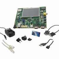
KIT EVAL FOR AT91SAMG45/9M10
Manufacturer
Atmel
Series
AT91SAM Smart ARMr
Type
MCUr
Specifications of AT91SAM9M10-G45-EK
Contents
Board, Cables, Power Supply
Processor To Be Evaluated
AT91SAM9M10
Processor Series
AT91SAM9
Data Bus Width
32 bit
Interface Type
RS-232, Ethernet, USB, JTAG
Operating Supply Voltage
5 V
Silicon Manufacturer
Atmel
Core Architecture
AVR
Kit Contents
Board
Features
Two High Speed USB Hosts, LCD TFT Display
Svhc
No SVHC (15-Dec-2010)
Mcu Supported Families
AT91SAM9M10,
Rohs Compliant
Yes
For Use With/related Products
AT91SAM9M10
Lead Free Status / RoHS Status
Lead free / RoHS Compliant
Available stocks
Company
Part Number
Manufacturer
Quantity
Price
Company:

Part Number:
AT91SAM9M10-G45-EK
Manufacturer:
INFINEON
Quantity:
10 000
Company:
Part Number:
AT91SAM9M10-G45-EK
Manufacturer:
Atmel
Quantity:
135


9.7.2.2
9.7.2.3
9.7.2.4
6355B–ATARM–21-Jun-10
Write Buffer
Write-though Operation
Write-back Operation
cache line is replaced due to a linefill or a cache clean operation, the dirty bits are used to decide
whether all, half or none is written back to memory.
DCache can be enabled or disabled by writing either 1 or 0 to bit C in register 1 of CP15 (see
Tables 4-3 and 4-4 on page 4-5 in ARM926EJ-S TRM).
The DCache supports write-through and write-back cache operations, selected by memory
region using the C and B bits in the MMU translation tables.
The DCache contains an eight data word entry, single address entry write-back buffer used to
hold write-back data for cache line eviction or cleaning of dirty cache lines.
The Write Buffer can hold up to 16 words of data and four separate addresses. DCache and
Write Buffer operations are closely connected as their configuration is set in each section by the
page descriptor in the MMU translation table.
The ARM926EJ-S contains a write buffer that has a 16-word data buffer and a four- address buf-
fer. The write buffer is used for all writes to a bufferable region, write-through region and write-
back region. It also allows to avoid stalling the processor when writes to external memory are
performed. When a store occurs, data is written to the write buffer at core speed (high speed).
The write buffer then completes the store to external memory at bus speed (typically slower than
the core speed). During this time, the ARM9EJ-S processor can preform other tasks.
DCache and Write Buffer support write-back and write-through memory regions, controlled by C
and B bits in each section and page descriptor within the MMU translation tables.
When a cache write hit occurs, the DCache line is updated. The updated data is then written to
the write buffer which transfers it to external memory.
When a cache write miss occurs, a line, chosen by round robin or another algorithm, is stored in
the write buffer which transfers it to external memory.
When a cache write hit occurs, the cache line or half line is marked as dirty, meaning that its
contents are not up-to-date with those in the external memory.
When a cache write miss occurs, a line, chosen by round robin or another algorithm, is stored in
the write buffer which transfers it to external memory.
AT91SAM9M10
47
Related parts for AT91SAM9M10-G45-EK
Image
Part Number
Description
Manufacturer
Datasheet
Request
R

Part Number:
Description:
KIT EVAL FOR AT91SAM9M10
Manufacturer:
Atmel
Datasheet:

Part Number:
Description:
IC MCU 16/32BIT ARM9 324TFBGA
Manufacturer:
Atmel
Datasheet:

Part Number:
Description:
At91 Arm Thumb-based Microcontrollers
Manufacturer:
ATMEL Corporation
Datasheet:

Part Number:
Description:
MCU, MPU & DSP Development Tools KICKSTART KIT FOR AT91SAM9 PLUS
Manufacturer:
IAR Systems

Part Number:
Description:
DEV KIT FOR AVR/AVR32
Manufacturer:
Atmel
Datasheet:
Part Number:
Description:
INTERVAL AND WIPE/WASH WIPER CONTROL IC WITH DELAY
Manufacturer:
ATMEL Corporation
Datasheet:
Part Number:
Description:
Low-Voltage Voice-Switched IC for Hands-Free Operation
Manufacturer:
ATMEL Corporation
Datasheet:
Part Number:
Description:
MONOLITHIC INTEGRATED FEATUREPHONE CIRCUIT
Manufacturer:
ATMEL Corporation
Datasheet:
Part Number:
Description:
AM-FM Receiver IC U4255BM-M
Manufacturer:
ATMEL Corporation
Datasheet:
Part Number:
Description:
Monolithic Integrated Feature Phone Circuit
Manufacturer:
ATMEL Corporation
Datasheet:
Part Number:
Description:
Multistandard Video-IF and Quasi Parallel Sound Processing
Manufacturer:
ATMEL Corporation
Datasheet:
Part Number:
Description:
High-performance EE PLD
Manufacturer:
ATMEL Corporation
Datasheet: