AT91SAM9M10-G45-EK Atmel, AT91SAM9M10-G45-EK Datasheet - Page 765
AT91SAM9M10-G45-EK
Manufacturer Part Number
AT91SAM9M10-G45-EK
Description
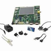
KIT EVAL FOR AT91SAMG45/9M10
Manufacturer
Atmel
Series
AT91SAM Smart ARMr
Type
MCUr
Specifications of AT91SAM9M10-G45-EK
Contents
Board, Cables, Power Supply
Processor To Be Evaluated
AT91SAM9M10
Processor Series
AT91SAM9
Data Bus Width
32 bit
Interface Type
RS-232, Ethernet, USB, JTAG
Operating Supply Voltage
5 V
Silicon Manufacturer
Atmel
Core Architecture
AVR
Kit Contents
Board
Features
Two High Speed USB Hosts, LCD TFT Display
Svhc
No SVHC (15-Dec-2010)
Mcu Supported Families
AT91SAM9M10,
Rohs Compliant
Yes
For Use With/related Products
AT91SAM9M10
Lead Free Status / RoHS Status
Lead free / RoHS Compliant
Available stocks
Company
Part Number
Manufacturer
Quantity
Price
Company:

Part Number:
AT91SAM9M10-G45-EK
Manufacturer:
INFINEON
Quantity:
10 000
Company:
Part Number:
AT91SAM9M10-G45-EK
Manufacturer:
Atmel
Quantity:
135


36.4
36.4.1
36.4.2
6355B–ATARM–21-Jun-10
Functional Description
Clock
Memory Interface
The MACB has several clock domains:
The system bus clock must run at least as fast as the receive clock and transmit clock (25 MHz
at 100 Mbps, and 2.5 MHZ at 10 Mbps).
Figure 36-1
The control registers drive the MDIO interface, setup up DMA activity, start frame transmission
and select modes of operation such as full- or half-duplex.
The receive block checks for valid preamble, FCS, alignment and length, and presents received
frames to the address checking block and DMA interface.
The transmit block takes data from the DMA interface, adds preamble and, if necessary, pad
and FCS, and transmits data according to the CSMA/CD (carrier sense multiple access with col-
lision detect) protocol. The start of transmission is deferred if CRS (carrier sense) is active.
If COL (collision) becomes active during transmission, a jam sequence is asserted and the
transmission is retried after a random back off. CRS and COL have no effect in full duplex mode.
The DMA block connects to external memory through its AHB bus interface. It contains receive
and transmit FIFOs for buffering frame data. It loads the transmit FIFO and empties the receive
FIFO using AHB bus master operations. Receive data is not sent to memory until the address
checking logic has determined that the frame should be copied. Receive or transmit frames are
stored in one or more buffers. Receive buffers have a fixed length of 128 bytes. Transmit buffers
range in length between 0 and 2047 bytes, and up to 128 buffers are permitted per frame. The
DMA block manages the transmit and receive framebuffer queues. These queues can hold mul-
tiple frames.
Synchronization module in the EMAC requires that the bus clock (hclk) runs at the speed of the
macb_tx/rx_clk at least, which is 25 MHz at 100 Mbps, and 2.5 MHz at 10 Mbps.
Frame data is transferred to and from the EMAC through the DMA interface. All transfers are 32-
bit words and may be single accesses or bursts of 2, 3 or 4 words. Burst accesses do not cross
sixteen-byte boundaries. Bursts of 4 words are the default data transfer; single accesses or
bursts of less than four words may be used to transfer data at the beginning or the end of a
buffer.
The DMA controller performs six types of operation on the bus. In order of priority, these are:
•
•
•
1. Receive buffer manager write
2. Receive buffer manager read
3. Transmit data DMA read
4. Receive data DMA write
5. Transmit buffer manager read
6. Transmit buffer manager write
System bus clock (AHB and APB): DMA and register blocks
Transmit clock: transmit block
Receive clock: receive and address checker block
illustrates the different blocks of the EMAC module.
AT91SAM9M10
765
Related parts for AT91SAM9M10-G45-EK
Image
Part Number
Description
Manufacturer
Datasheet
Request
R

Part Number:
Description:
KIT EVAL FOR AT91SAM9M10
Manufacturer:
Atmel
Datasheet:

Part Number:
Description:
IC MCU 16/32BIT ARM9 324TFBGA
Manufacturer:
Atmel
Datasheet:

Part Number:
Description:
At91 Arm Thumb-based Microcontrollers
Manufacturer:
ATMEL Corporation
Datasheet:

Part Number:
Description:
MCU, MPU & DSP Development Tools KICKSTART KIT FOR AT91SAM9 PLUS
Manufacturer:
IAR Systems

Part Number:
Description:
DEV KIT FOR AVR/AVR32
Manufacturer:
Atmel
Datasheet:
Part Number:
Description:
INTERVAL AND WIPE/WASH WIPER CONTROL IC WITH DELAY
Manufacturer:
ATMEL Corporation
Datasheet:
Part Number:
Description:
Low-Voltage Voice-Switched IC for Hands-Free Operation
Manufacturer:
ATMEL Corporation
Datasheet:
Part Number:
Description:
MONOLITHIC INTEGRATED FEATUREPHONE CIRCUIT
Manufacturer:
ATMEL Corporation
Datasheet:
Part Number:
Description:
AM-FM Receiver IC U4255BM-M
Manufacturer:
ATMEL Corporation
Datasheet:
Part Number:
Description:
Monolithic Integrated Feature Phone Circuit
Manufacturer:
ATMEL Corporation
Datasheet:
Part Number:
Description:
Multistandard Video-IF and Quasi Parallel Sound Processing
Manufacturer:
ATMEL Corporation
Datasheet:
Part Number:
Description:
High-performance EE PLD
Manufacturer:
ATMEL Corporation
Datasheet: