C8051F350DK Silicon Laboratories Inc, C8051F350DK Datasheet - Page 123
C8051F350DK
Manufacturer Part Number
C8051F350DK
Description
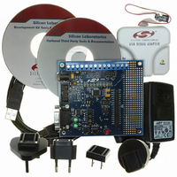
DEV KIT FOR F350/351/352/353
Manufacturer
Silicon Laboratories Inc
Type
MCUr
Specifications of C8051F350DK
Contents
Evaluation Board, Power Supply, USB Cables, Adapter and Documentation
Processor To Be Evaluated
C8051F35x
Interface Type
USB
Silicon Manufacturer
Silicon Labs
Core Architecture
8051
Silicon Core Number
C8051F350
Silicon Family Name
C8051F35x
Lead Free Status / RoHS Status
Contains lead / RoHS non-compliant
For Use With/related Products
C8051F350, 351, 352, 353
Lead Free Status / Rohs Status
Lead free / RoHS Compliant
Other names
336-1083
Available stocks
Company
Part Number
Manufacturer
Quantity
Price
Company:

Part Number:
C8051F350DK
Manufacturer:
SiliconL
Quantity:
8


15.2. Non-volatile Data Storage
The Flash memory can be used for non-volatile data storage as well as program code. This allows data
such as calibration coefficients to be calculated and stored at run time. Data is written using the MOVX
write instruction and read using the MOVC instruction. Note: MOVX read instructions always target XRAM.
15.3. Security Options
The CIP-51 provides security options to protect the Flash memory from inadvertent modification by soft-
ware as well as to prevent the viewing of proprietary program code and constants. The Program Store
Write Enable (bit PSWE in register PSCTL) and the Program Store Erase Enable (bit PSEE in register
PSCTL) bits protect the Flash memory from accidental modification by software. PSWE must be explicitly
set to ‘1’ before software can modify the Flash memory; both PSWE and PSEE must be set to ‘1’ before
software can erase Flash memory. Additional security features prevent proprietary program code and data
constants from being read or altered across the C2 interface.
A Security Lock Byte located at the last byte of Flash user space offers protection of the Flash program
memory from access (reads, writes, or erases) by unprotected code or the C2 interface. The Flash security
mechanism allows the user to lock n 512-byte Flash pages, starting at page 0 (addresses 0x0000 to
0x01FF), where n is the 1’s complement number represented by the Security Lock Byte. Note that the
page containing the Flash Security Lock Byte is locked when any other Flash pages are locked. See exam-
ple below.
Flash pages locked:
Security Lock Byte:
Addresses locked:
1’s Complement:
other Flash pages are
according to the Flash
Locked when any
security lock byte
Access limit set
locked
Figure 15.1. Flash Memory Map
Unlocked Flash Pages
0x0000 to 0x03FF (first two Flash pages) and
3 (First two Flash pages + Lock Byte Page)
Lock Byte
Reserved
0x1C00 to 0x1DFF (Lock Byte Page)
Rev. 1.1
00000010b
11111101b
0x1E00
0x1DFF
0x1DFE
0x1C00
0x0000
C8051F350/1/2/3
Flash memory organized
in 512-byte pages
123
Related parts for C8051F350DK
Image
Part Number
Description
Manufacturer
Datasheet
Request
R

Part Number:
Description:
SMD/C°/SINGLE-ENDED OUTPUT SILICON OSCILLATOR
Manufacturer:
Silicon Laboratories Inc
Part Number:
Description:
Manufacturer:
Silicon Laboratories Inc
Datasheet:
Part Number:
Description:
N/A N/A/SI4010 AES KEYFOB DEMO WITH LCD RX
Manufacturer:
Silicon Laboratories Inc
Datasheet:
Part Number:
Description:
N/A N/A/SI4010 SIMPLIFIED KEY FOB DEMO WITH LED RX
Manufacturer:
Silicon Laboratories Inc
Datasheet:
Part Number:
Description:
N/A/-40 TO 85 OC/EZLINK MODULE; F930/4432 HIGH BAND (REV E/B1)
Manufacturer:
Silicon Laboratories Inc
Part Number:
Description:
EZLink Module; F930/4432 Low Band (rev e/B1)
Manufacturer:
Silicon Laboratories Inc
Part Number:
Description:
I°/4460 10 DBM RADIO TEST CARD 434 MHZ
Manufacturer:
Silicon Laboratories Inc
Part Number:
Description:
I°/4461 14 DBM RADIO TEST CARD 868 MHZ
Manufacturer:
Silicon Laboratories Inc
Part Number:
Description:
I°/4463 20 DBM RFSWITCH RADIO TEST CARD 460 MHZ
Manufacturer:
Silicon Laboratories Inc
Part Number:
Description:
I°/4463 20 DBM RADIO TEST CARD 868 MHZ
Manufacturer:
Silicon Laboratories Inc
Part Number:
Description:
I°/4463 27 DBM RADIO TEST CARD 868 MHZ
Manufacturer:
Silicon Laboratories Inc
Part Number:
Description:
I°/4463 SKYWORKS 30 DBM RADIO TEST CARD 915 MHZ
Manufacturer:
Silicon Laboratories Inc
Part Number:
Description:
N/A N/A/-40 TO 85 OC/4463 RFMD 30 DBM RADIO TEST CARD 915 MHZ
Manufacturer:
Silicon Laboratories Inc
Part Number:
Description:
I°/4463 20 DBM RADIO TEST CARD 169 MHZ
Manufacturer:
Silicon Laboratories Inc