C8051F350DK Silicon Laboratories Inc, C8051F350DK Datasheet - Page 31
C8051F350DK
Manufacturer Part Number
C8051F350DK
Description
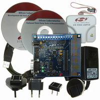
DEV KIT FOR F350/351/352/353
Manufacturer
Silicon Laboratories Inc
Type
MCUr
Specifications of C8051F350DK
Contents
Evaluation Board, Power Supply, USB Cables, Adapter and Documentation
Processor To Be Evaluated
C8051F35x
Interface Type
USB
Silicon Manufacturer
Silicon Labs
Core Architecture
8051
Silicon Core Number
C8051F350
Silicon Family Name
C8051F35x
Lead Free Status / RoHS Status
Contains lead / RoHS non-compliant
For Use With/related Products
C8051F350, 351, 352, 353
Lead Free Status / Rohs Status
Lead free / RoHS Compliant
Other names
336-1083
Available stocks
Company
Part Number
Manufacturer
Quantity
Price
Company:

Part Number:
C8051F350DK
Manufacturer:
SiliconL
Quantity:
8


4.
DGND
XTAL1
XTAL2
AGND
Pinout and Package Definitions
Name
C2CK
P2.0/
P0.2/
P0.3/
/RST
P0.0
P0.1
P0.4
P0.5
C2D
V
AV+
DD
Pin Numbers
‘F350
‘F352
21
22
10
12
11
13
14
15
16
17
18
Table 4.1. Pin Definitions for the C8051F350/1/2/3
9
‘F351
‘F353
17
18
10
11
12
13
14
6
5
8
7
9
D I/O or
D I/O or
D I/O or
A I/O or
D I/O or
D I/O or
Ground Digital Ground. Must be tied to Ground.
Ground Analog Ground. Must be tied to Ground.
Power
Power
D I/O
D I/O
D I/O
D I/O
D I/O
Type
A In
A In
A In
A In
D In
A In
A In
Description
Digital Supply Voltage. Must be tied to +2.7 V to +3.6 V
power.
Analog Supply Voltage. Must be tied to +2.7 V to +3.6 V
power.
Device Reset. Open-drain output of internal POR or V
monitor. An external source can initiate a system reset by
driving this pin low for at least 15 µs. A 1kΩ pull-up to V
recommended. See Reset Sources Section.
Clock signal for the C2 Debug Interface.
Port 2.0. See Port I/O Section for a complete description.
Bi-directional data signal for the C2 Debug Interface.
Port 0.0. See Port I/O Section for a complete description.
Port 0.1. See Port I/O Section for a complete description.
Port 0.2. See Port I/O Section for a complete description.
This pin is the external oscillator return for a crystal or reso-
nator. See Oscillator Section.
Port 0.3. See Port I/O Section for a complete description.
This pin is the excitation driver for an external crystal or res-
onator, or an external clock input for CMOS, capacitor, or
RC oscillator configurations. See Oscillator Section.
Port 0.4. See Port I/O Section for a complete description.
Port 0.5. See Port I/O Section for a complete description.
Rev. 1.1
C8051F350/1/2/3
DD
DD
is
31
Related parts for C8051F350DK
Image
Part Number
Description
Manufacturer
Datasheet
Request
R

Part Number:
Description:
SMD/C°/SINGLE-ENDED OUTPUT SILICON OSCILLATOR
Manufacturer:
Silicon Laboratories Inc
Part Number:
Description:
Manufacturer:
Silicon Laboratories Inc
Datasheet:
Part Number:
Description:
N/A N/A/SI4010 AES KEYFOB DEMO WITH LCD RX
Manufacturer:
Silicon Laboratories Inc
Datasheet:
Part Number:
Description:
N/A N/A/SI4010 SIMPLIFIED KEY FOB DEMO WITH LED RX
Manufacturer:
Silicon Laboratories Inc
Datasheet:
Part Number:
Description:
N/A/-40 TO 85 OC/EZLINK MODULE; F930/4432 HIGH BAND (REV E/B1)
Manufacturer:
Silicon Laboratories Inc
Part Number:
Description:
EZLink Module; F930/4432 Low Band (rev e/B1)
Manufacturer:
Silicon Laboratories Inc
Part Number:
Description:
I°/4460 10 DBM RADIO TEST CARD 434 MHZ
Manufacturer:
Silicon Laboratories Inc
Part Number:
Description:
I°/4461 14 DBM RADIO TEST CARD 868 MHZ
Manufacturer:
Silicon Laboratories Inc
Part Number:
Description:
I°/4463 20 DBM RFSWITCH RADIO TEST CARD 460 MHZ
Manufacturer:
Silicon Laboratories Inc
Part Number:
Description:
I°/4463 20 DBM RADIO TEST CARD 868 MHZ
Manufacturer:
Silicon Laboratories Inc
Part Number:
Description:
I°/4463 27 DBM RADIO TEST CARD 868 MHZ
Manufacturer:
Silicon Laboratories Inc
Part Number:
Description:
I°/4463 SKYWORKS 30 DBM RADIO TEST CARD 915 MHZ
Manufacturer:
Silicon Laboratories Inc
Part Number:
Description:
N/A N/A/-40 TO 85 OC/4463 RFMD 30 DBM RADIO TEST CARD 915 MHZ
Manufacturer:
Silicon Laboratories Inc
Part Number:
Description:
I°/4463 20 DBM RADIO TEST CARD 169 MHZ
Manufacturer:
Silicon Laboratories Inc