C8051F350DK Silicon Laboratories Inc, C8051F350DK Datasheet - Page 171
C8051F350DK
Manufacturer Part Number
C8051F350DK
Description
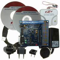
DEV KIT FOR F350/351/352/353
Manufacturer
Silicon Laboratories Inc
Type
MCUr
Specifications of C8051F350DK
Contents
Evaluation Board, Power Supply, USB Cables, Adapter and Documentation
Processor To Be Evaluated
C8051F35x
Interface Type
USB
Silicon Manufacturer
Silicon Labs
Core Architecture
8051
Silicon Core Number
C8051F350
Silicon Family Name
C8051F35x
Lead Free Status / RoHS Status
Contains lead / RoHS non-compliant
For Use With/related Products
C8051F350, 351, 352, 353
Lead Free Status / Rohs Status
Lead free / RoHS Compliant
Other names
336-1083
Available stocks
Company
Part Number
Manufacturer
Quantity
Price
Company:

Part Number:
C8051F350DK
Manufacturer:
SiliconL
Quantity:
8


20. UART0
UART0 is an asynchronous, full duplex serial port offering modes 1 and 3 of the standard 8051 UART.
Enhanced baud rate support allows a wide range of clock sources to generate standard baud rates (details
in Section “20.1. Enhanced Baud Rate Generation’ on page 172). Received data buffering allows UART0
to start reception of a second incoming data byte before software has finished reading the previous data
byte.
UART0 has two associated SFRs: Serial Control Register 0 (SCON0) and Serial Data Buffer 0 (SBUF0).
The single SBUF0 location provides access to both transmit and receive registers. Writes to SBUF0
always access the Transmit register. Reads of SBUF0 always access the buffered Receive register;
it is not possible to read data from the Transmit register.
With UART0 interrupts enabled, an interrupt is generated each time a transmit is completed (TI0 is set in
SCON0), or a data byte has been received (RI0 is set in SCON0). The UART0 interrupt flags are not
cleared by hardware when the CPU vectors to the interrupt service routine. They must be cleared manually
by software, allowing software to determine the cause of the UART0 interrupt (transmit complete or receive
complete).
Rate Generator
UART Baud
Write to
SBUF
Figure 20.1. UART0 Block Diagram
Rx Clock
Tx Clock
Stop Bit
Start
Start
SBUF
Read
SCON
D
TB8
SET
CLR
Shift
Input Shift Register
Q
Shift
SFR Bus
(RX Latch)
(9 bits)
Tx Control
Rx Control
SBUF
0x1FF
SFR Bus
Zero Detector
(TX Shift)
SBUF
Rev. 1.1
RB8
Load SBUF
Tx IRQ
Rx IRQ
RI
TI
SBUF
Load
Send
Data
Interrupt
Serial
Port
RX
TX
C8051F350/1/2/3
Crossbar
Crossbar
Port I/O
171
Related parts for C8051F350DK
Image
Part Number
Description
Manufacturer
Datasheet
Request
R

Part Number:
Description:
SMD/C°/SINGLE-ENDED OUTPUT SILICON OSCILLATOR
Manufacturer:
Silicon Laboratories Inc
Part Number:
Description:
Manufacturer:
Silicon Laboratories Inc
Datasheet:
Part Number:
Description:
N/A N/A/SI4010 AES KEYFOB DEMO WITH LCD RX
Manufacturer:
Silicon Laboratories Inc
Datasheet:
Part Number:
Description:
N/A N/A/SI4010 SIMPLIFIED KEY FOB DEMO WITH LED RX
Manufacturer:
Silicon Laboratories Inc
Datasheet:
Part Number:
Description:
N/A/-40 TO 85 OC/EZLINK MODULE; F930/4432 HIGH BAND (REV E/B1)
Manufacturer:
Silicon Laboratories Inc
Part Number:
Description:
EZLink Module; F930/4432 Low Band (rev e/B1)
Manufacturer:
Silicon Laboratories Inc
Part Number:
Description:
I°/4460 10 DBM RADIO TEST CARD 434 MHZ
Manufacturer:
Silicon Laboratories Inc
Part Number:
Description:
I°/4461 14 DBM RADIO TEST CARD 868 MHZ
Manufacturer:
Silicon Laboratories Inc
Part Number:
Description:
I°/4463 20 DBM RFSWITCH RADIO TEST CARD 460 MHZ
Manufacturer:
Silicon Laboratories Inc
Part Number:
Description:
I°/4463 20 DBM RADIO TEST CARD 868 MHZ
Manufacturer:
Silicon Laboratories Inc
Part Number:
Description:
I°/4463 27 DBM RADIO TEST CARD 868 MHZ
Manufacturer:
Silicon Laboratories Inc
Part Number:
Description:
I°/4463 SKYWORKS 30 DBM RADIO TEST CARD 915 MHZ
Manufacturer:
Silicon Laboratories Inc
Part Number:
Description:
N/A N/A/-40 TO 85 OC/4463 RFMD 30 DBM RADIO TEST CARD 915 MHZ
Manufacturer:
Silicon Laboratories Inc
Part Number:
Description:
I°/4463 20 DBM RADIO TEST CARD 169 MHZ
Manufacturer:
Silicon Laboratories Inc