C8051F350DK Silicon Laboratories Inc, C8051F350DK Datasheet - Page 8
C8051F350DK
Manufacturer Part Number
C8051F350DK
Description
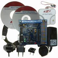
DEV KIT FOR F350/351/352/353
Manufacturer
Silicon Laboratories Inc
Type
MCUr
Specifications of C8051F350DK
Contents
Evaluation Board, Power Supply, USB Cables, Adapter and Documentation
Processor To Be Evaluated
C8051F35x
Interface Type
USB
Silicon Manufacturer
Silicon Labs
Core Architecture
8051
Silicon Core Number
C8051F350
Silicon Family Name
C8051F35x
Lead Free Status / RoHS Status
Contains lead / RoHS non-compliant
For Use With/related Products
C8051F350, 351, 352, 353
Lead Free Status / Rohs Status
Lead free / RoHS Compliant
Other names
336-1083
Available stocks
Company
Part Number
Manufacturer
Quantity
Price
Company:

Part Number:
C8051F350DK
Manufacturer:
SiliconL
Quantity:
8


C8051F350/1/2/3
11. Memory Organization and SFRs
12. Interrupt Handler
13. Prefetch Engine
14. Reset Sources
15. Flash Memory
16. External RAM
17. Oscillators
18. Port Input/Output
19. SMBus
20. UART0
21. Serial Peripheral Interface (SPI0)
8
Figure 11.1. Memory Map ........................................................................................ 99
Figure 14.1. Reset Sources.................................................................................... 115
Figure 14.2. Power-On and VDD Monitor Reset Timing ........................................ 116
Figure 15.1. Flash Memory Map............................................................................. 123
Figure 17.1. Oscillator Diagram.............................................................................. 129
Figure 17.2. 32.768 kHz External Crystal Example................................................ 132
Figure 18.1. Port I/O Functional Block Diagram ..................................................... 137
Figure 18.2. Port I/O Cell Block Diagram ............................................................... 138
Figure 18.3. Crossbar Priority Decoder with No Pins Skipped ............................... 139
Figure 18.4. Crossbar Priority Decoder with Crystal Pins Skipped ........................ 140
Figure 19.1. SMBus Block Diagram ....................................................................... 151
Figure 19.2. Typical SMBus Configuration ............................................................. 152
Figure 19.3. SMBus Transaction ............................................................................ 153
Figure 19.4. Typical SMBus SCL Generation......................................................... 157
Figure 19.5. Typical Master Transmitter Sequence................................................ 163
Figure 19.6. Typical Master Receiver Sequence.................................................... 164
Figure 19.7. Typical Slave Receiver Sequence...................................................... 165
Figure 19.8. Typical Slave Transmitter Sequence.................................................. 166
Figure 20.1. UART0 Block Diagram ....................................................................... 171
Figure 20.2. UART0 Baud Rate Logic .................................................................... 172
Figure 20.3. UART Interconnect Diagram .............................................................. 173
Figure 20.4. 8-Bit UART Timing Diagram............................................................... 173
Figure 20.5. 9-Bit UART Timing Diagram............................................................... 174
Figure 20.6. UART Multi-Processor Mode Interconnect Diagram .......................... 175
Figure 21.1. SPI Block Diagram ............................................................................. 181
Figure 21.2. Multiple-Master Mode Connection Diagram ....................................... 184
Figure 21.3. 3-Wire Single Master and Slave Mode Connection Diagram ............. 184
Figure 21.4. 4-Wire Single Master and Slave Mode Connection Diagram ............. 184
Figure 21.5. Data/Clock Timing Relationship ......................................................... 186
Figure 21.6. SPI Master Timing (CKPHA = 0)........................................................ 191
Figure 21.7. SPI Master Timing (CKPHA = 1)........................................................ 191
Figure 21.8. SPI Slave Timing (CKPHA = 0).......................................................... 192
Figure 21.9. SPI Slave Timing (CKPHA = 1).......................................................... 192
Rev. 1.1
Related parts for C8051F350DK
Image
Part Number
Description
Manufacturer
Datasheet
Request
R

Part Number:
Description:
SMD/C°/SINGLE-ENDED OUTPUT SILICON OSCILLATOR
Manufacturer:
Silicon Laboratories Inc
Part Number:
Description:
Manufacturer:
Silicon Laboratories Inc
Datasheet:
Part Number:
Description:
N/A N/A/SI4010 AES KEYFOB DEMO WITH LCD RX
Manufacturer:
Silicon Laboratories Inc
Datasheet:
Part Number:
Description:
N/A N/A/SI4010 SIMPLIFIED KEY FOB DEMO WITH LED RX
Manufacturer:
Silicon Laboratories Inc
Datasheet:
Part Number:
Description:
N/A/-40 TO 85 OC/EZLINK MODULE; F930/4432 HIGH BAND (REV E/B1)
Manufacturer:
Silicon Laboratories Inc
Part Number:
Description:
EZLink Module; F930/4432 Low Band (rev e/B1)
Manufacturer:
Silicon Laboratories Inc
Part Number:
Description:
I°/4460 10 DBM RADIO TEST CARD 434 MHZ
Manufacturer:
Silicon Laboratories Inc
Part Number:
Description:
I°/4461 14 DBM RADIO TEST CARD 868 MHZ
Manufacturer:
Silicon Laboratories Inc
Part Number:
Description:
I°/4463 20 DBM RFSWITCH RADIO TEST CARD 460 MHZ
Manufacturer:
Silicon Laboratories Inc
Part Number:
Description:
I°/4463 20 DBM RADIO TEST CARD 868 MHZ
Manufacturer:
Silicon Laboratories Inc
Part Number:
Description:
I°/4463 27 DBM RADIO TEST CARD 868 MHZ
Manufacturer:
Silicon Laboratories Inc
Part Number:
Description:
I°/4463 SKYWORKS 30 DBM RADIO TEST CARD 915 MHZ
Manufacturer:
Silicon Laboratories Inc
Part Number:
Description:
N/A N/A/-40 TO 85 OC/4463 RFMD 30 DBM RADIO TEST CARD 915 MHZ
Manufacturer:
Silicon Laboratories Inc
Part Number:
Description:
I°/4463 20 DBM RADIO TEST CARD 169 MHZ
Manufacturer:
Silicon Laboratories Inc