TOOLSTICK540DC Silicon Laboratories Inc, TOOLSTICK540DC Datasheet - Page 165
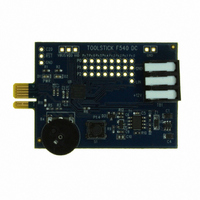
TOOLSTICK540DC
Manufacturer Part Number
TOOLSTICK540DC
Description
DAUGHTER CARD TOOLSTICK F540
Manufacturer
Silicon Laboratories Inc
Series
ToolStickr
Type
MCUr
Datasheets
1.TOOLSTICK540DC.pdf
(274 pages)
2.TOOLSTICK540DC.pdf
(16 pages)
3.TOOLSTICK540DC.pdf
(12 pages)
Specifications of TOOLSTICK540DC
Contents
Daughter Card
Processor To Be Evaluated
C8051F54x
Processor Series
C8051F54x
Interface Type
USB
Operating Supply Voltage
2.7 V to 3.6 V
Lead Free Status / RoHS Status
Lead free / RoHS Compliant
For Use With/related Products
C8051F54x
For Use With
336-1345 - TOOLSTICK BASE ADAPTER336-1182 - ADAPTER USB DEBUG FOR C8051FXXX
Lead Free Status / Rohs Status
Lead free / RoHS Compliant
Other names
336-1717


SFR Definition 18.19. P1SKIP: Port 1 Skip
SFR Address = 0xD5; SFR Page = 0x0F
SFR Definition 18.20. P2: Port 2
SFR Address = 0xA0; SFR Page = All Pages; Bit-Addressable
Note: P2.2-P2.7 are only available on the 32-pin packages.
Name
Reset
Name
Reset
Bit
7:0
Bit
7:0
Type
Type
Bit
Bit
P1SKIP[7:0]
P2[7:0]
Name
Name
7
0
7
1
Port 2Data.
Sets the Port latch logic
value or reads the Port pin
logic state in Port cells con-
figured for digital I/O.
Port 1 Crossbar Skip Enable Bits.
These bits select Port 1 pins to be skipped by the Crossbar Decoder. Port pins
used for analog, special functions or GPIO should be skipped by the Crossbar.
0: Corresponding P1.n pin is not skipped by the Crossbar.
1: Corresponding P1.n pin is skipped by the Crossbar.
6
0
6
1
Description
5
0
5
1
Rev. 1.1
0: Set output latch to logic
LOW.
1: Set output latch to logic
HIGH.
4
0
4
1
P1SKIP[7:0]
P2[7:0]
R/W
R/W
Function
Write
3
0
3
1
2
0
2
1
0: P2.n Port pin is logic
LOW.
1: P2.n Port pin is logic
HIGH.
C8051F54x
1
0
1
1
Read
0
0
0
1
165
Related parts for TOOLSTICK540DC
Image
Part Number
Description
Manufacturer
Datasheet
Request
R

Part Number:
Description:
KIT TOOL EVAL SYS IN A USB STICK
Manufacturer:
Silicon Laboratories Inc
Datasheet:

Part Number:
Description:
TOOLSTICK DEBUG ADAPTER
Manufacturer:
Silicon Laboratories Inc
Datasheet:

Part Number:
Description:
TOOLSTICK BASE ADAPTER
Manufacturer:
Silicon Laboratories Inc
Datasheet:

Part Number:
Description:
TOOLSTICK DAUGHTER CARD
Manufacturer:
Silicon Laboratories Inc
Datasheet:

Part Number:
Description:
TOOLSTICK DAUGHTER CARD
Manufacturer:
Silicon Laboratories Inc
Datasheet:

Part Number:
Description:
TOOLSTICK DAUGHTER CARD
Manufacturer:
Silicon Laboratories Inc
Datasheet:

Part Number:
Description:
TOOLSTICK PROGRAMMING ADAPTER
Manufacturer:
Silicon Laboratories Inc
Datasheet:

Part Number:
Description:
TOOLSTICK DAUGHTER CARD
Manufacturer:
Silicon Laboratories Inc
Datasheet:

Part Number:
Description:
KIT STARTER TOOLSTICK
Manufacturer:
Silicon Laboratories Inc
Datasheet:

Part Number:
Description:
KIT UNIVERSITY TOOLSTICK STARTER
Manufacturer:
Silicon Laboratories Inc
Datasheet:

Part Number:
Description:
DAUGHTER CARD TOOLSTICK F330
Manufacturer:
Silicon Laboratories Inc
Datasheet:

Part Number:
Description:
CARD DAUGHTER UNIVRSTY TOOLSTICK
Manufacturer:
Silicon Laboratories Inc
Datasheet:

Part Number:
Description:
DAUGHTER CARD TOOLSTICK F582
Manufacturer:
Silicon Laboratories Inc
Datasheet:

Part Number:
Description:
DAUGHTER CARD TOOLSTICK F500
Manufacturer:
Silicon Laboratories Inc
Datasheet:

Part Number:
Description:
DAUGHTER CARD TOOLSTICK F560
Manufacturer:
Silicon Laboratories Inc
Datasheet: