HW-V5-ML550-UNI-G Xilinx Inc, HW-V5-ML550-UNI-G Datasheet - Page 31
HW-V5-ML550-UNI-G
Manufacturer Part Number
HW-V5-ML550-UNI-G
Description
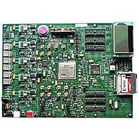
EVALUATION PLATFORM VIRTEX-5
Manufacturer
Xilinx Inc
Series
Virtex™-5 LXTr
Type
FPGAr
Datasheet
1.HW-V5-ML550-UNI-G.pdf
(88 pages)
Specifications of HW-V5-ML550-UNI-G
Contents
Development Platform, Power Supply, Loopback Board, CompactFlash Card, software and documentation
Silicon Manufacturer
Xilinx
Features
64M X 8 DDR SDRAM Memory, Six Samtec LVDS Connectors
Kit Contents
Board, Cable, PSU, CD, Docs
Silicon Family Name
Virtex-5
Silicon Core Number
XC5VLX50T-FFG1136
Rohs Compliant
Yes
Lead Free Status / RoHS Status
Lead free / RoHS Compliant
For Use With/related Products
Virtex™-5 LXT
Lead Free Status / RoHS Status
Lead free / RoHS Compliant, Lead free / RoHS Compliant
Available stocks
Company
Part Number
Manufacturer
Quantity
Price


ML550 Networking Interfaces Platform
UG202 (v1.4) April 18, 2008
C
5V
IN
R
Important Note About ± 5% Margin Limits
Inhibit
Jumper
2
3
Table 3-11: VR_SEL[3:0] FPGA Pinout
The ML550 Networking Interfaces Platform implements the remote ±5% output
adjustment using two Maxim analog mux devices: an 8-to-1 for the margin R
and a 2-to-1 to select between the output of the 8-to-1 mux or the R
the voltage regulator output to its nominal value. These analog muxes have analog switch
resistance on the order of 1 . Each voltage regulator has its own independent margin
control capabilities as shown in
schematic for voltage regulator control.
Xilinx devices are specified to work over ±5% power rail variations. In
outer margin resistors in the ±10% and ±7.5% locations are set to the value which gives
±5% regulator output. Any changes to these resistor values that allow the regulator output
to exceed ±5% will void the board warranty.
Figure 3-9
Each regulator has similar margin control circuitry, only the Radj resistors vary between
regulators. A pull-down resistor is tied to the FPGA_RESETB signal so that the default
“nominal” regulator output value is selected at board power-up (before the FPGA has been
configured). The normally closed switch in the 2-to-1 mux selects the “nominal” output
adjustment resistor (R
V
INHIBIT
IN
Regulator
Figure 3-8: Typical Voltage Regulator Configuration
Voltage
GND
1
VR_SEL[3:0]
V
VR_SEL0
VR_SEL1
VR_SEL2
VR_SEL3
O_ADJ
shows typical margin control circuit details.
V
Signal
OUT
5
4
V
Details: Figure 3-9
ADJ
Control Circuit
NOM
See Margin
www.xilinx.com
).
Figure 3-8
C
FPGA
OUT
Pin #
AE7
AE6
W6
Y6
and
Figure
1
2
Voltage Regulators (TI PTH05000)
3-9.
Test
Point
Connector
Figure 3-8
NOM
shows a typical
G
Figure
resistor that sets
3.3V
D
S
UG202_3_08_050906
ADJ
3-9, the two
Power
On
LED
selection
V
OUT
31
Related parts for HW-V5-ML550-UNI-G
Image
Part Number
Description
Manufacturer
Datasheet
Request
R

Part Number:
Description:
IC CPLD .8K 36MCELL 44-VQFP
Manufacturer:
Xilinx Inc
Datasheet:

Part Number:
Description:
IC CPLD 72MCRCELL 10NS 44VQFP
Manufacturer:
Xilinx Inc
Datasheet:

Part Number:
Description:
IC CPLD 1.6K 72MCELL 64-VQFP
Manufacturer:
Xilinx Inc
Datasheet:

Part Number:
Description:
IC CR-II CPLD 64MCELL 44-VQFP
Manufacturer:
Xilinx Inc
Datasheet:

Part Number:
Description:
IC CPLD 1.6K 72MCELL 100-TQFP
Manufacturer:
Xilinx Inc
Datasheet:

Part Number:
Description:
IC CR-II CPLD 64MCELL 56-BGA
Manufacturer:
Xilinx Inc
Datasheet:

Part Number:
Description:
IC CPLD 72MCRCELL 7.5NS 44VQFP
Manufacturer:
Xilinx Inc
Datasheet:
Part Number:
Description:
IC CR-II CPLD 64MCELL 100-VQFP
Manufacturer:
Xilinx Inc
Datasheet:
Part Number:
Description:
IC CPLD 1.6K 72MCELL 100-TQFP
Manufacturer:
Xilinx Inc
Datasheet:

Part Number:
Description:
IC CPLD 72MCRCELL 7.5NS 64VQFP
Manufacturer:
Xilinx Inc
Datasheet:
Part Number:
Description:
IC CPLD 1.6K 72MCELL 100-TQFP
Manufacturer:
Xilinx Inc
Datasheet:

Part Number:
Description:
IC CPLD 1.5K 64MCELL HP 44-VQFP
Manufacturer:
Xilinx Inc

Part Number:
Description:
IC CPLD 36MCRCELL 15NS 44PLCC
Manufacturer:
Xilinx Inc
Datasheet:

Part Number:
Description:
IC CPLD 36MCRCELL 10NS 44PLCC
Manufacturer:
Xilinx Inc
Datasheet:

Part Number:
Description:
IC CPLD 1.5K 64MCELL HP 44-VQFP
Manufacturer:
Xilinx Inc