HW-V5-ML550-UNI-G Xilinx Inc, HW-V5-ML550-UNI-G Datasheet - Page 73
HW-V5-ML550-UNI-G
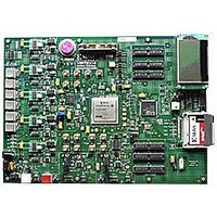
Manufacturer Part Number
HW-V5-ML550-UNI-G
Description
EVALUATION PLATFORM VIRTEX-5
Manufacturer
Xilinx Inc
Series
Virtex™-5 LXTr
Type
FPGAr
Datasheet
1.HW-V5-ML550-UNI-G.pdf
(88 pages)
Specifications of HW-V5-ML550-UNI-G
Contents
Development Platform, Power Supply, Loopback Board, CompactFlash Card, software and documentation
Silicon Manufacturer
Xilinx
Features
64M X 8 DDR SDRAM Memory, Six Samtec LVDS Connectors
Kit Contents
Board, Cable, PSU, CD, Docs
Silicon Family Name
Virtex-5
Silicon Core Number
XC5VLX50T-FFG1136
Rohs Compliant
Yes
Lead Free Status / RoHS Status
Lead free / RoHS Compliant
For Use With/related Products
Virtex™-5 LXT
Lead Free Status / RoHS Status
Lead free / RoHS Compliant, Lead free / RoHS Compliant
Available stocks
Company
Part Number
Manufacturer
Quantity
Price


ML550 Networking Interfaces Platform
UG202 (v1.4) April 18, 2008
Operation Example of the 64128EFCBC-3LP
R
The voltage and contrast settings must be configured before the LCD panel is ready for
operation.
controller.
The KS0713 LCD controller has several default settings of operation on the LCD panel
display PCB. Some settings are forced through direct bonding on the chip. The default
settings are:
ADC Select
- ADC = 0 SEG1 --> SEG132
- ADC = 1 SEG132 --> SEG1
SHL Select
- SHL = 0 COM1 --> COM64
- SHL = 1 COM64 --> COM1
Master mode
Parallel mode
Internal oscillator
Duty cycle ratio is set to 1/65
Voltage converter input is between 2.4V VDD 3.6V, where VDD connects to 3.3V
Internal voltage divider resistors
Temperature coefficient is set to -0.05%/ C
Figure C-6
Figure C-6: LCD Controller Initialization Flow
shows the initialization procedure required to set up the LCD
FPGA Configured and Application Running
www.xilinx.com
RESETB Pin is Taken HIGH
RESETB Pin is Kept LOW
Board Power Supply Start
RESETB Pin is Kept LOW
Start FPGA Configuration
Regulator Resistor Select
Set Reference Voltage
Setup Instruction Flow
Voltage Converter ON
Voltage Regulator ON
Voltage Follower ON
LCD Bias Select
End Initialization
ADC Select
SHL Select
Power ON
Setting Reference Voltage
is a two-pass instruction:
- Set Reference Voltage Mode
- Set Reference Voltage Register
LCD Bias
DUTY0, 1 is "11".
LCD Bias 0 = 1/7
LCD Bias 1 = 1/9
than 1 ms to let the voltages stabilize.
The on-chip resistors are used.
Therefore, the selection MUST be
set to 101.
Wait between each instruction longer
Hardware Schematic Diagram
UG202_C_06_050906
73
Related parts for HW-V5-ML550-UNI-G
Image
Part Number
Description
Manufacturer
Datasheet
Request
R

Part Number:
Description:
IC CPLD .8K 36MCELL 44-VQFP
Manufacturer:
Xilinx Inc
Datasheet:

Part Number:
Description:
IC CPLD 72MCRCELL 10NS 44VQFP
Manufacturer:
Xilinx Inc
Datasheet:

Part Number:
Description:
IC CPLD 1.6K 72MCELL 64-VQFP
Manufacturer:
Xilinx Inc
Datasheet:

Part Number:
Description:
IC CR-II CPLD 64MCELL 44-VQFP
Manufacturer:
Xilinx Inc
Datasheet:

Part Number:
Description:
IC CPLD 1.6K 72MCELL 100-TQFP
Manufacturer:
Xilinx Inc
Datasheet:

Part Number:
Description:
IC CR-II CPLD 64MCELL 56-BGA
Manufacturer:
Xilinx Inc
Datasheet:

Part Number:
Description:
IC CPLD 72MCRCELL 7.5NS 44VQFP
Manufacturer:
Xilinx Inc
Datasheet:
Part Number:
Description:
IC CR-II CPLD 64MCELL 100-VQFP
Manufacturer:
Xilinx Inc
Datasheet:
Part Number:
Description:
IC CPLD 1.6K 72MCELL 100-TQFP
Manufacturer:
Xilinx Inc
Datasheet:

Part Number:
Description:
IC CPLD 72MCRCELL 7.5NS 64VQFP
Manufacturer:
Xilinx Inc
Datasheet:
Part Number:
Description:
IC CPLD 1.6K 72MCELL 100-TQFP
Manufacturer:
Xilinx Inc
Datasheet:

Part Number:
Description:
IC CPLD 1.5K 64MCELL HP 44-VQFP
Manufacturer:
Xilinx Inc

Part Number:
Description:
IC CPLD 36MCRCELL 15NS 44PLCC
Manufacturer:
Xilinx Inc
Datasheet:

Part Number:
Description:
IC CPLD 36MCRCELL 10NS 44PLCC
Manufacturer:
Xilinx Inc
Datasheet:

Part Number:
Description:
IC CPLD 1.5K 64MCELL HP 44-VQFP
Manufacturer:
Xilinx Inc