EVAL-ADUC814QS Analog Devices Inc, EVAL-ADUC814QS Datasheet - Page 11
EVAL-ADUC814QS
Manufacturer Part Number
EVAL-ADUC814QS
Description
KIT DEV FOR ADUC814 QUICK START
Manufacturer
Analog Devices Inc
Series
QuickStart™ Kitr
Type
8052-corer
Datasheet
1.EVAL-ADUC814QSZ.pdf
(72 pages)
Specifications of EVAL-ADUC814QS
Contents
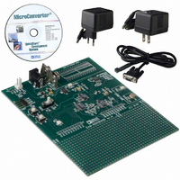
Evaluation Board, Power Supply, Cable, Software and Documentation
For Use With/related Products
ADuC814
Lead Free Status / RoHS Status
Contains lead / RoHS non-compliant


Pin No.
17
18–21
18
19
20
21
22–24
22
22
23
24
25
26
27
28
I = Input, O = Output, S = Supply, G - Ground.
The following notes apply to the entire data sheet:
•
•
•
In bit designation tables, set implies a Logic 1 state, and cleared implies a Logic 0 state, unless otherwise stated.
Set and cleared also imply that the bit is set or cleared by the ADuC814 hardware, unless otherwise stated.
User software should not write to reserved or unimplemented bits as they may be used in future products.
Mnemonic
C
P1.4–P1.7
P1.4/ADC2
P1.5/ADC3
P1.6/ADC4/
DAC0
P1.7/
ADC5/DAC1
P3.5–P3.7
P3.5/T1
P3.5/ SS
/EXTCLK
P3.6/MISO
P3.7/SDATA/
MOSI
SCLOCK
XTAL1
XTAL2
DV
REF
DD
Type
I
I
I
I
I/O
I/O
I/O
I/O
I/O
I/O
I/O
I
O
S
Function
Decoupling Input for On-Chip Reference. Connect 0.1 µF between this pin and AGND.
Port 1.4 to P1.7. These pins have no digital output drivers, i.e., they can only function as digital inputs,
for which 0 must be written to the port bit. These port pins also have the following analog functionality:
ADC Input Channel 2. Selected via ADCCON2 SFR.
ADC Input Channel 2. Selected via ADCCON2 SFR.
ADC Input Channel 4. Selected via ADCCON2 SFR. The voltage DAC Channel 0 can also be configured
to appear on P1.6.
ADC Input Channel 5, selected via ADCCON2 SFR. The voltage DAC Channel 1 can also be configured
to appear on P1.7.
Bidirectional Port Pins with Internal Pull-Up Resistors. Port 3 pins that have 1s written to them are
pulled high by the internal pull-up resistors, and in that state they can be used as inputs. As inputs
,with Port 3 pins being pulled low externally, they source current because of the internal pull-up
resistors. When driving a 0-to-1 output transition a strong pull-up is active during S1 of the instruction
cycle. Port 3 pins also have various secondary functions which are described as follows.
I/O Timer/Counter 1 Input. P3.5–P3.7 pins also have SPI interface functions. To enable these functions,
Bit 0 of the CFG814 SFR must be set to 1.
This pin also functions as the Slave Select input for the SPI interface when the device is operated in
slave mode. P3.5 can also function as an input for an external clock. This clock effectively bypasses the
PLL. This function is enabled by setting Bit 1 of the CFG814 SFR.
SPI Master Input/Slave Output Data Input/Output Pin.
SPI Master Output/Slave Input Data Input/Output Pin.
Serial Clock Pin for SPI Serial Interface Clock.
Input to the Crystal Oscillator Inverter.
Output from the Crystal Oscillator Inverter.
Analog Positive Supply Voltage, 3 V or 5 V.
Rev. A | Page 11 of 72
ADuC814
Related parts for EVAL-ADUC814QS
Image
Part Number
Description
Manufacturer
Datasheet
Request
R


Part Number:
Description:
BOARD EVAL FOR SI270X-A
Manufacturer:
Silicon Laboratories Inc
Datasheet:

Part Number:
Description:
BUCK CONV REF DESIGN KIT IP1201
Manufacturer:
International Rectifier
Datasheet:
Part Number:
Description:
BOARD DEMO SYNC DUAL BUCK CNVTER
Manufacturer:
International Rectifier
Datasheet:
Part Number:
Description:
BOARD DEMO SYNC BUCK CONVETER
Manufacturer:
International Rectifier
Datasheet:

Part Number:
Description:
EVALBOARD/EB Omnidirectional microphone - Analog
Manufacturer:
Analog Devices
Datasheet:
Part Number:
Description:
EVALBOARD/EB Omnidirectional microphone - Analog
Manufacturer:
Analog Devices
Datasheet:


Part Number:
Description:
BOARD EVAL LED DRIVER LT3756
Manufacturer:
Linear Technology
Datasheet:

Part Number:
Description:
BOARD EVAL FOR AD7741/7742
Manufacturer:
Analog Devices Inc
Datasheet:

Part Number:
Description:
±1.7g Dual-Axis IMEMS Accelerometer Evaluation Board
Manufacturer:
Analog Devices Inc
Datasheet:

Part Number:
Description:
IC MULTIPLIER ANALOG 8-SOIC T/R
Manufacturer:
Analog Devices Inc
Datasheet:

Part Number:
Description:
IC ANALOG MULTIPLIER 8-DIP
Manufacturer:
Analog Devices Inc
Datasheet:
Part Number:
Description:
IC ANALOG MULTIPLIER 8-SOIC
Manufacturer:
Analog Devices Inc
Datasheet:
Part Number:
Description:
IC ANALOG MULTIPLIER 8-DIP
Manufacturer:
Analog Devices Inc
Datasheet: