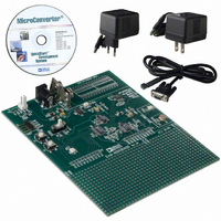
EVAL-ADUC814QS Analog Devices Inc, EVAL-ADUC814QS Datasheet - Page 54

EVAL-ADUC814QS
Manufacturer Part Number
EVAL-ADUC814QS
Description
KIT DEV FOR ADUC814 QUICK START
Manufacturer
Analog Devices Inc
Series
QuickStart™ Kitr
Type
8052-corer
Datasheet
1.EVAL-ADUC814QSZ.pdf
(72 pages)
Specifications of EVAL-ADUC814QS
Contents
Evaluation Board, Power Supply, Cable, Software and Documentation
For Use With/related Products
ADuC814
Lead Free Status / RoHS Status
Contains lead / RoHS non-compliant
ADuC814
Mode 0: 8-Bit Shift Register Mode
Mode 0 is selected by clearing both the SM0 and SM1 bits in the
SFR SCON. Serial data enters and exits through RxD. TxD
outputs the shift clock. Eight data bits are transmitted or
received. Transmission is initiated by any instruction that writes
to SBUF. The data is shifted out of the RxD line. The eight bits
are transmitted with the least-significant bit (LSB) first, as
shown in Figure 52.
Reception is initiated when the receive enable bit (REN) is 1
and the receive interrupt bit (RI) is 0. When RI is cleared the
data is clocked into the RxD line and the clock pulses are output
from the TxD line.
Mode 1: 8-Bit UART, Variable Baud Rate
Mode 1 is selected by clearing SM0 and setting SM1. Each data
byte (LSB first) is preceded by a start bit (Bit 0) and followed by
a stop bit (Bit 1). Therefore 10 bits are transmitted on TxD or
received on RxD. The baud rate is set by the Timer 1 or Timer 2
overflow rate, or a combination of the two (one for transmission
and the other for reception).
Transmission is initiated by writing to SBUF. The write-to-
SBUF signal also loads a 1 (stop bit) into the ninth bit position
of the transmit shift register. The data is output bit by bit until
the stop bit appears on TxD and the transmit interrupt flag (TI)
is automatically set as shown in Figure 51.
(SHIFT CLOCK)
(DATA OUT)
CORE
CLK
ALE
RxD
TxD
S1
S2
MACHINE
DATA BIT 0
CYCLE 1
S3
Figure 52. UART Serial Port Transmission, Mode 0
S4
S5
S6
Rev. A | Page 54 of 72
S1
DATA BIT 1
S2
MACHINE
CYCLE 2
S3
S4
Reception is initiated when a 1-to-0 transition is detected on
RxD. Assuming a valid start bit was detected, character
reception continues. The start bit is skipped and the eight data
bits are clocked into the serial port shift register. When all eight
bits have been clocked in, the following events occur:
•
•
(SCON. 1)
MACHINE
CYCLE 7
DATA BIT 6
The eight bits in the receive shift register are latched into
SBUF.
The ninth bit (stop bit) is clocked into RB8 in SCON. The
receiver interrupt flag (RI) is set if, and only if, the
following conditions are met at the time the final shift
pulse is generated:
o
o
If either of these conditions is not met, the received frame
is irretrievably lost, and RI is not set.
TxD
S4
TI
S5
START
RI = 0
Either SM2 = 0 or SM2 = 1 and
the received stop bit = 1
BIT
S6
Figure 51. UART Serial Port Transmission, Mode 1
S1
D0
S2
DATA BIT 7
D1
MACHINE
CYCLE 8
S3
D2
S4
S5
D3
S6
D4
D5
I.E., READY FOR MORE DATA
D6
SET INTERRUPT
D7
STOP BIT


