EVAL-ADUC814QS Analog Devices Inc, EVAL-ADUC814QS Datasheet - Page 35
EVAL-ADUC814QS
Manufacturer Part Number
EVAL-ADUC814QS
Description
KIT DEV FOR ADUC814 QUICK START
Manufacturer
Analog Devices Inc
Series
QuickStart™ Kitr
Type
8052-corer
Datasheet
1.EVAL-ADUC814QSZ.pdf
(72 pages)
Specifications of EVAL-ADUC814QS
Contents
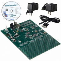
Evaluation Board, Power Supply, Cable, Software and Documentation
For Use With/related Products
ADuC814
Lead Free Status / RoHS Status
Contains lead / RoHS non-compliant


DACxH/L
Function
SFR Address
Power-On Default
Bit Addressable
The 12-bit DAC data should be written into DACxH/L right-justified such that DACL contains the lower eight bits, and the lower nibble
of DACH contains the upper four bits.
Using the DACs
The on-chip DAC architecture consists of a resistor string DAC
followed by an output buffer amplifier, the functional equivalent
of which is illustrated in Figure 38. Features of this architecture
include inherent guaranteed monotonicity and excellent differ-
ential linearity.
As illustrated in Figure 38, the reference source for each DAC is
user selectable in software. It can be either AV
0 V-to-AV
from 0 V to the voltage at the AV
the DAC output transfer function spans from 0 V to the internal
V
pin. The DAC output buffer features a true rail-to-rail output
stage implementation. This means that, unloaded, each output is
capable of swinging to within less than 100 mV of both AV
and ground. Moreover, the DAC’s linearity specification (when
driving a 10 kΩ resistive load to ground) is guaranteed through
the full transfer function except Codes 0 to 48, and, in 0 V-to-
AV
near ground and V
buffer, and a general representation of its effects (neglecting
offset and gain error) is illustrated in Figure 39. The dotted line
in Figure 39 indicates the ideal transfer function, and the solid
line represents what the transfer function might look like with
endpoint nonlinearities due to saturation of the output buffer.
Note that Figure 39 represents a transfer function in 0 V-to-V
mode only. In 0 V-to-V
REF
DD
, or if an external reference is applied, the voltage at the V
mode only, Codes 3945 to 4095. Linearity degradation
AV
Figure 38. Resistor String DAC Functional Equivalent
DD
V
REF
DD
mode, the DAC output transfer function spans
DD
R
R
R
R
R
is caused by saturation of the output
REF
ADuC814
mode (with V
DAC0 and DAC1 Data Registers
DAC Data Registers, written by the user to update the DAC outputs.
DAC0L (DAC0 data low byte) –> F9H DAC0H (DAC0 data high byte) –> FAH;
DAC1L (DAC1 data low byte) –> FBH DAC1H (DAC1 data high byte) –> FCH
00H –> Both DAC0 and DAC1 data registers.
No –> Both DAC0 and DAC1 data registers.
DD
pin. In 0 V-to-V
(FROM MCU)
DISABLE
OUTPUT
BUFFER
HIGH Z
REF
< V
DD
DD
or V
), the lower
DAC0
REF
REF
mode,
. In
DD
Rev. A | Page 35 of 72
REF
DD
nonlinearity would be similar, but the upper portion of the
transfer function would follow the ideal line right to the end
(V
linearity error.
V
The endpoint nonlinearities conceptually illustrated in Figure 39
get worse as a function of output loading. Most ADuC814
specifications assume a 10 kΩ resistive load to ground at the
DAC output. As the output is forced to source or sink more
current, the nonlinear regions at the top or bottom (respectively)
of Figure 39 become larger. With larger current demands, this
can significantly limit output voltage swing. Figure 40 and
Figure 41 illustrate this behavior. Note that the upper trace in
each of these figures is valid only for an output range selection
of 0 V-to-AV
cause high-side voltage drops as long as the reference voltage
remains below the upper trace in the corresponding figure. For
example, if AV
not affected by loads less than 5 mA. But around 7 mA, the
upper curve in Figure 41 drops below 2.5 V (V
that at these higher currents the output cannot reach V
V
DD
DD
REF
–100mV
–50mV
100mV
50mV
0mV
in this case, not V
V
Figure 39. Endpoint Nonlinearities Due to Amplifier Saturation
DD
000H
DD
DD
. In 0 V-to-V
= 3 V and V
DD
), showing no signs of upper endpoint
REF
REF
mode, DAC loading does not
= 2.5 V, the high-side voltage is
REF
), indicating
ADuC814
REF
.
FFFH
Related parts for EVAL-ADUC814QS
Image
Part Number
Description
Manufacturer
Datasheet
Request
R


Part Number:
Description:
BOARD EVAL FOR SI270X-A
Manufacturer:
Silicon Laboratories Inc
Datasheet:

Part Number:
Description:
BUCK CONV REF DESIGN KIT IP1201
Manufacturer:
International Rectifier
Datasheet:
Part Number:
Description:
BOARD DEMO SYNC DUAL BUCK CNVTER
Manufacturer:
International Rectifier
Datasheet:
Part Number:
Description:
BOARD DEMO SYNC BUCK CONVETER
Manufacturer:
International Rectifier
Datasheet:

Part Number:
Description:
EVALBOARD/EB Omnidirectional microphone - Analog
Manufacturer:
Analog Devices
Datasheet:
Part Number:
Description:
EVALBOARD/EB Omnidirectional microphone - Analog
Manufacturer:
Analog Devices
Datasheet:


Part Number:
Description:
BOARD EVAL LED DRIVER LT3756
Manufacturer:
Linear Technology
Datasheet:

Part Number:
Description:
BOARD EVAL FOR AD7741/7742
Manufacturer:
Analog Devices Inc
Datasheet:

Part Number:
Description:
±1.7g Dual-Axis IMEMS Accelerometer Evaluation Board
Manufacturer:
Analog Devices Inc
Datasheet:

Part Number:
Description:
IC MULTIPLIER ANALOG 8-SOIC T/R
Manufacturer:
Analog Devices Inc
Datasheet:

Part Number:
Description:
IC ANALOG MULTIPLIER 8-DIP
Manufacturer:
Analog Devices Inc
Datasheet:
Part Number:
Description:
IC ANALOG MULTIPLIER 8-SOIC
Manufacturer:
Analog Devices Inc
Datasheet:
Part Number:
Description:
IC ANALOG MULTIPLIER 8-DIP
Manufacturer:
Analog Devices Inc
Datasheet: