PIC18LF13K22-I/P Microchip Technology, PIC18LF13K22-I/P Datasheet - Page 104
PIC18LF13K22-I/P
Manufacturer Part Number
PIC18LF13K22-I/P
Description
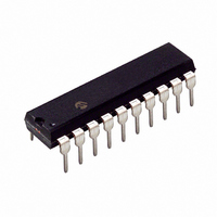
IC PIC MCU FLASH 256KX8 20-PDIP
Manufacturer
Microchip Technology
Series
PIC® XLP™ 18Fr
Datasheets
1.PIC18LF13K22-ISS.pdf
(388 pages)
2.PIC18LF13K22-ISS.pdf
(12 pages)
3.PIC18LF13K22-ISS.pdf
(36 pages)
4.PIC18LF14K22-IP.pdf
(382 pages)
Specifications of PIC18LF13K22-I/P
Program Memory Type
FLASH
Program Memory Size
8KB (4K x 16)
Package / Case
20-DIP (0.300", 7.62mm)
Core Processor
PIC
Core Size
8-Bit
Speed
64MHz
Connectivity
I²C, LIN, SPI, UART/USART
Peripherals
Brown-out Detect/Reset, POR, PWM, WDT
Number Of I /o
17
Eeprom Size
256 x 8
Ram Size
256 x 8
Voltage - Supply (vcc/vdd)
1.8 V ~ 3.6 V
Data Converters
A/D 12x10b
Oscillator Type
Internal
Operating Temperature
-40°C ~ 85°C
Processor Series
PIC18LF
Core
PIC
Data Bus Width
8 bit
Data Ram Size
256 B
Interface Type
I2C, MSSP, SPI, USART
Maximum Clock Frequency
32 KHz
Number Of Programmable I/os
18
Number Of Timers
4
Operating Supply Voltage
1.8 V to 3.6 V
Maximum Operating Temperature
+ 125 C
Mounting Style
Through Hole
3rd Party Development Tools
52715-96, 52716-328, 52717-734, 52712-325, EWPIC18
Development Tools By Supplier
PG164130, DV164035, DV244005, DV164005
Minimum Operating Temperature
- 40 C
On-chip Adc
10 bit, 12 Channel
Lead Free Status / RoHS Status
Lead free / RoHS Compliant
Lead Free Status / RoHS Status
Lead free / RoHS Compliant, Lead free / RoHS Compliant


PIC18F1XK22/LF1XK22
10.2
Timer1 can be configured for 16-bit reads and writes
(see Figure 10-2). When the RD16 control bit of the
T1CON register is set, the address for TMR1H is
mapped to a buffer register for the high byte of Timer1.
A read from TMR1L will load the contents of the high
byte of Timer1 into the Timer1 high byte buffer. This
provides the user with the ability to accurately read all
16 bits of Timer1 without the need to determine
whether a read of the high byte, followed by a read of
the low byte, has become invalid due to a rollover or
carry between reads.
Writing to TMR1H does not directly affect Timer1.
Instead, the high byte of Timer1 is updated with the
contents of TMR1H when a write occurs to TMR1L.
This allows all 16 bits of Timer1 to be updated at once.
The high byte of Timer1 is not directly readable or
writable in this mode. All reads and writes must take
place through the Timer1 High Byte Buffer register.
Writes to TMR1H do not clear the Timer1 prescaler.
The prescaler is only cleared on writes to TMR1L.
10.3
The TMR1CS bit of the T1CON register is used to select
the clock source. When TMR1CS = 0, the clock source
is F
supplied externally.
10.3.1
When the internal clock source is selected the
TMR1H:TMR1L register pair will increment on multiples
of F
10.3.2
When the external clock source is selected, the Timer1
module may work as a timer or a counter.
When counting, Timer1 is incremented on the rising
edge of the external clock input T1CKI. In addition, the
Counter mode clock can be synchronized to the
microcontroller system clock or run asynchronously.
DS41365D-page 104
F
T1CKI pin
T1LPOSC
OSC
Source
Clock
OSC
OSC
/4
/4. When TMR1CS = 1, the clock source is
as determined by the Timer1 prescaler.
Timer1 16-Bit Read/Write Mode
Clock Source Selection
INTERNAL CLOCK SOURCE
EXTERNAL CLOCK SOURCE
T1OSCEN
x
0
1
INTOSCIO
FOSC
Mode
LP or
xxx
xxx
TMR1CS
0
1
1
Preliminary
If an external clock oscillator is needed (and the
microcontroller is using the INTOSC without CLKOUT),
Timer1 can use the LP oscillator as a clock source.
10.4
An on-chip crystal oscillator circuit is incorporated
between pins OSC1 (input) and OSC2 (amplifier output).
It is enabled by setting the Timer1 Oscillator Enable bit,
T1OSCEN of the T1CON register. The oscillator is a
low-power circuit rated for 32 kHz crystals. It will
continue to run during all power-managed modes. The
circuit for a typical LP oscillator is shown in Figure 10-3.
Table 10-1 shows the capacitor selection for the Timer1
oscillator.
The Timer1 oscillator is shared with the system LP
oscillator. Thus, Timer1 can use this mode only when
the primary system clock is derived from the internal
oscillator or when the oscillator is in the LP mode. The
user must provide a software time delay to ensure
proper oscillator start-up.
FIGURE 10-3:
Note:
Note:
Note:
Timer1 Oscillator
27 pF
27 pF
C1
C2
• Timer1 enabled after POR
• Write to TMR1H or TMR1L
• Timer1 is disabled
• Timer1 is disabled (TMR1ON 0) when
In Counter mode, a falling edge must be
registered by the counter prior to the first
incrementing rising edge after any one or
more of the following conditions:
See Figure 9-2.
See the Notes with Table 10-1 for additional
information about capacitor selection.
T1CKI is high then Timer1 is enabled
(TMR1ON=1) when T1CKI is low.
32.768 kHz
XTAL
EXTERNAL
COMPONENTS FOR THE
TIMER1 LP OSCILLATOR
2010 Microchip Technology Inc.
OSC1
OSC2
PIC
®
MCU
Related parts for PIC18LF13K22-I/P
Image
Part Number
Description
Manufacturer
Datasheet
Request
R

Part Number:
Description:
Manufacturer:
Microchip Technology Inc.
Datasheet:
Part Number:
Description:
Manufacturer:
Microchip Technology Inc.
Datasheet:
Part Number:
Description:
Manufacturer:
Microchip Technology Inc.
Datasheet:
Part Number:
Description:
Manufacturer:
Microchip Technology Inc.
Datasheet:
Part Number:
Description:
Manufacturer:
Microchip Technology Inc.
Datasheet:
Part Number:
Description:
Manufacturer:
Microchip Technology Inc.
Datasheet:
Part Number:
Description:
Manufacturer:
Microchip Technology Inc.
Datasheet:
Part Number:
Description:
Manufacturer:
Microchip Technology Inc.
Datasheet: