PIC18LF13K22-I/P Microchip Technology, PIC18LF13K22-I/P Datasheet - Page 378
PIC18LF13K22-I/P
Manufacturer Part Number
PIC18LF13K22-I/P
Description
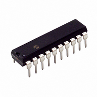
IC PIC MCU FLASH 256KX8 20-PDIP
Manufacturer
Microchip Technology
Series
PIC® XLP™ 18Fr
Datasheets
1.PIC18LF13K22-ISS.pdf
(388 pages)
2.PIC18LF13K22-ISS.pdf
(12 pages)
3.PIC18LF13K22-ISS.pdf
(36 pages)
4.PIC18LF14K22-IP.pdf
(382 pages)
Specifications of PIC18LF13K22-I/P
Program Memory Type
FLASH
Program Memory Size
8KB (4K x 16)
Package / Case
20-DIP (0.300", 7.62mm)
Core Processor
PIC
Core Size
8-Bit
Speed
64MHz
Connectivity
I²C, LIN, SPI, UART/USART
Peripherals
Brown-out Detect/Reset, POR, PWM, WDT
Number Of I /o
17
Eeprom Size
256 x 8
Ram Size
256 x 8
Voltage - Supply (vcc/vdd)
1.8 V ~ 3.6 V
Data Converters
A/D 12x10b
Oscillator Type
Internal
Operating Temperature
-40°C ~ 85°C
Processor Series
PIC18LF
Core
PIC
Data Bus Width
8 bit
Data Ram Size
256 B
Interface Type
I2C, MSSP, SPI, USART
Maximum Clock Frequency
32 KHz
Number Of Programmable I/os
18
Number Of Timers
4
Operating Supply Voltage
1.8 V to 3.6 V
Maximum Operating Temperature
+ 125 C
Mounting Style
Through Hole
3rd Party Development Tools
52715-96, 52716-328, 52717-734, 52712-325, EWPIC18
Development Tools By Supplier
PG164130, DV164035, DV244005, DV164005
Minimum Operating Temperature
- 40 C
On-chip Adc
10 bit, 12 Channel
Lead Free Status / RoHS Status
Lead free / RoHS Compliant
Lead Free Status / RoHS Status
Lead free / RoHS Compliant, Lead free / RoHS Compliant


PIC18F1XK22/LF1XK22
I
ID Locations .............................................................. 261, 276
INCF.................................................................................. 298
INCFSZ ............................................................................. 299
In-Circuit Debugger ........................................................... 276
In-Circuit Serial Programming (ICSP) ....................... 261, 276
Indexed Literal Offset Addressing
Indexed Literal Offset Mode .............................................. 324
Indirect Addressing ............................................................. 44
INFSNZ ............................................................................. 299
Initialization Conditions for all Registers ........................... 257
Instruction Cycle.................................................................. 31
Instruction Flow/Pipelining .................................................. 31
Instruction Set ................................................................... 277
DS41365D-page 378
2
C Mode (MSSP)
Acknowledge Sequence Timing................................ 170
Baud Rate Generator ................................................ 163
Bus Collision
Clock Arbitration........................................................ 164
Clock Stretching ........................................................ 156
Clock Synchronization and the CKP bit (SEN = 1) ... 157
Effects of a Reset...................................................... 171
General Call Address Support .................................. 160
I
Master Mode ............................................................. 161
Multi-Master Communication, Bus Collision and
Multi-Master Mode .................................................... 171
Operation .................................................................. 148
Read/Write Bit Information (R/W Bit) ................ 148, 149
Registers ................................................................... 144
Serial Clock (RC3/SCK/SCL) .................................... 149
Slave Mode ............................................................... 148
Sleep Operation ........................................................ 171
Stop Condition Timing............................................... 170
and Standard PIC18 Instructions .............................. 324
Clocking Scheme ........................................................ 31
ADDLW ..................................................................... 283
ADDWF ..................................................................... 283
ADDWF (Indexed Literal Offset Mode) ..................... 325
ADDWFC .................................................................. 284
ANDLW ..................................................................... 284
ANDWF ..................................................................... 285
BC ............................................................................. 285
BCF ........................................................................... 286
BN ............................................................................. 286
BNC .......................................................................... 287
BNN .......................................................................... 287
BNOV ........................................................................ 288
BNZ ........................................................................... 288
BOV .......................................................................... 291
BRA........................................................................... 289
2
C Clock Rate w/BRG .............................................. 163
During a Repeated Start Condition ................... 174
During a Stop Condition.................................... 176
10-Bit Slave Receive Mode (SEN = 1).............. 156
10-Bit Slave Transmit Mode.............................. 156
7-Bit Slave Receive Mode (SEN = 1)................ 156
7-Bit Slave Transmit Mode................................ 156
Operation .......................................................... 162
Reception.......................................................... 167
Repeated Start Condition Timing...................... 166
Start Condition Timing ...................................... 165
Transmission..................................................... 167
Arbitration.......................................................... 171
Addressing ........................................................ 148
Reception.......................................................... 149
Transmission..................................................... 149
Preliminary
INTCON Register................................................................ 67
INTCON Registers........................................................ 67–69
INTCON2 Register.............................................................. 68
INTCON3 Register.............................................................. 69
Inter-Integrated Circuit. See I
BSF........................................................................... 289
BSF (Indexed Literal Offset Mode) ........................... 325
BTFSC ...................................................................... 290
BTFSS ...................................................................... 290
BTG .......................................................................... 291
BZ ............................................................................. 292
CALL......................................................................... 292
CLRF ........................................................................ 293
CLRWDT .................................................................. 293
COMF ....................................................................... 294
CPFSEQ ................................................................... 294
CPFSGT ................................................................... 295
CPFSLT .................................................................... 295
DAW ......................................................................... 296
DCFSNZ ................................................................... 297
DECF ........................................................................ 296
DECFSZ ................................................................... 297
Extended Instruction Set .......................................... 319
General Format......................................................... 279
GOTO ....................................................................... 298
INCF ......................................................................... 298
INCFSZ..................................................................... 299
INFSNZ..................................................................... 299
IORLW ...................................................................... 300
IORWF...................................................................... 300
LFSR ........................................................................ 301
MOVF ....................................................................... 301
MOVFF ..................................................................... 302
MOVLB ..................................................................... 302
MOVLW .................................................................... 303
MOVWF .................................................................... 303
MULLW..................................................................... 304
MULWF..................................................................... 304
NEGF........................................................................ 305
NOP .......................................................................... 305
Opcode Field Descriptions........................................ 278
POP .......................................................................... 306
PUSH........................................................................ 306
RCALL ...................................................................... 307
RESET...................................................................... 307
RETFIE ..................................................................... 308
RETLW ..................................................................... 308
RETURN................................................................... 309
RLCF ........................................................................ 309
RLNCF...................................................................... 310
RRCF........................................................................ 310
RRNCF ..................................................................... 311
SETF ........................................................................ 311
SETF (Indexed Literal Offset Mode) ......................... 325
SLEEP ...................................................................... 312
SUBFWB .................................................................. 312
SUBLW ..................................................................... 313
SUBWF..................................................................... 313
SUBWFB .................................................................. 314
SWAPF ..................................................................... 314
TBLRD ...................................................................... 315
TBLWT ..................................................................... 316
TSTFSZ .................................................................... 317
XORLW .................................................................... 317
XORWF .................................................................... 318
2010 Microchip Technology Inc.
2
C.
Related parts for PIC18LF13K22-I/P
Image
Part Number
Description
Manufacturer
Datasheet
Request
R

Part Number:
Description:
Manufacturer:
Microchip Technology Inc.
Datasheet:
Part Number:
Description:
Manufacturer:
Microchip Technology Inc.
Datasheet:
Part Number:
Description:
Manufacturer:
Microchip Technology Inc.
Datasheet:
Part Number:
Description:
Manufacturer:
Microchip Technology Inc.
Datasheet:
Part Number:
Description:
Manufacturer:
Microchip Technology Inc.
Datasheet:
Part Number:
Description:
Manufacturer:
Microchip Technology Inc.
Datasheet:
Part Number:
Description:
Manufacturer:
Microchip Technology Inc.
Datasheet:
Part Number:
Description:
Manufacturer:
Microchip Technology Inc.
Datasheet: