PIC18LF13K22-I/P Microchip Technology, PIC18LF13K22-I/P Datasheet - Page 116
PIC18LF13K22-I/P
Manufacturer Part Number
PIC18LF13K22-I/P
Description
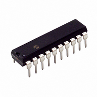
IC PIC MCU FLASH 256KX8 20-PDIP
Manufacturer
Microchip Technology
Series
PIC® XLP™ 18Fr
Datasheets
1.PIC18LF13K22-ISS.pdf
(388 pages)
2.PIC18LF13K22-ISS.pdf
(12 pages)
3.PIC18LF13K22-ISS.pdf
(36 pages)
4.PIC18LF14K22-IP.pdf
(382 pages)
Specifications of PIC18LF13K22-I/P
Program Memory Type
FLASH
Program Memory Size
8KB (4K x 16)
Package / Case
20-DIP (0.300", 7.62mm)
Core Processor
PIC
Core Size
8-Bit
Speed
64MHz
Connectivity
I²C, LIN, SPI, UART/USART
Peripherals
Brown-out Detect/Reset, POR, PWM, WDT
Number Of I /o
17
Eeprom Size
256 x 8
Ram Size
256 x 8
Voltage - Supply (vcc/vdd)
1.8 V ~ 3.6 V
Data Converters
A/D 12x10b
Oscillator Type
Internal
Operating Temperature
-40°C ~ 85°C
Processor Series
PIC18LF
Core
PIC
Data Bus Width
8 bit
Data Ram Size
256 B
Interface Type
I2C, MSSP, SPI, USART
Maximum Clock Frequency
32 KHz
Number Of Programmable I/os
18
Number Of Timers
4
Operating Supply Voltage
1.8 V to 3.6 V
Maximum Operating Temperature
+ 125 C
Mounting Style
Through Hole
3rd Party Development Tools
52715-96, 52716-328, 52717-734, 52712-325, EWPIC18
Development Tools By Supplier
PG164130, DV164035, DV244005, DV164005
Minimum Operating Temperature
- 40 C
On-chip Adc
10 bit, 12 Channel
Lead Free Status / RoHS Status
Lead free / RoHS Compliant
Lead Free Status / RoHS Status
Lead free / RoHS Compliant, Lead free / RoHS Compliant


PIC18F1XK22/LF1XK22
13.3
In Compare mode, the 16-bit CCPR1 register value is
constantly compared against either the TMR1 or TMR3
register pair value. When a match occurs, the CCP1
pin can be:
• driven high
• driven low
• toggled (high-to-low or low-to-high)
• remain unchanged (that is, reflects the state of the
The action on the pin is based on the value of the mode
select bits (CCP1M<3:0>). At the same time, the inter-
rupt flag bit, CCP1IF, is set.
13.3.1
The user must configure the CCP1 pin as an output by
clearing the appropriate TRIS bit.
FIGURE 13-2:
DS41365D-page 116
I/O latch)
Note:
Compare Mode
CCP PIN CONFIGURATION
Clearing the CCP1CON register will force
the CCP1 compare output latch (depend-
ing on device configuration) to the default
low level. This is not the PORTC I/O
DATA
0
1
latch.
T3CCP1
COMPARE MODE OPERATION BLOCK DIAGRAM
CCPR1H
TMR1H
TMR3H
Comparator
CCPR1L
TMR1L
TMR3L
Compare
Match
Preliminary
Set CCP1IF
(Timer1/Timer3 Reset, A/D Trigger)
13.3.2
Timer1 and/or Timer3 must be running in Timer mode
or Synchronized Counter mode if the CCP module is
using the compare feature. In Asynchronous Counter
mode, the compare operation will not work reliably.
13.3.3
When the Generate Software Interrupt mode is chosen
(CCP1M<3:0> = 1010), the CCP1 pin is not affected.
Only the CCP1IF interrupt flag is affected.
13.3.4
The CCP module is equipped with a Special Event
Trigger. This is an internal hardware signal generated
in Compare mode to trigger actions by other modules.
The Special Event Trigger is enabled by selecting
the
(CCP1M<3:0> = 1011).
The Special Event Trigger resets the timer register pair
for whichever timer resource is currently assigned as the
module’s time base. This allows the CCPR1 registers to
serve as a programmable period register for either timer.
The Special Event Trigger can also start an A/D con-
version. In order to do this, the A/D converter must
already be enabled.
Special Event Trigger
CCP1CON<3:0>
Compare
Output
Logic
4
TIMER1/TIMER3 MODE SELECTION
SOFTWARE INTERRUPT MODE
SPECIAL EVENT TRIGGER
Special
S
R
Q
2010 Microchip Technology Inc.
Output Enable
Event
TRIS
Trigger
CCP1 pin
mode
Related parts for PIC18LF13K22-I/P
Image
Part Number
Description
Manufacturer
Datasheet
Request
R

Part Number:
Description:
Manufacturer:
Microchip Technology Inc.
Datasheet:
Part Number:
Description:
Manufacturer:
Microchip Technology Inc.
Datasheet:
Part Number:
Description:
Manufacturer:
Microchip Technology Inc.
Datasheet:
Part Number:
Description:
Manufacturer:
Microchip Technology Inc.
Datasheet:
Part Number:
Description:
Manufacturer:
Microchip Technology Inc.
Datasheet:
Part Number:
Description:
Manufacturer:
Microchip Technology Inc.
Datasheet:
Part Number:
Description:
Manufacturer:
Microchip Technology Inc.
Datasheet:
Part Number:
Description:
Manufacturer:
Microchip Technology Inc.
Datasheet: