PIC18LF13K22-I/P Microchip Technology, PIC18LF13K22-I/P Datasheet - Page 239
PIC18LF13K22-I/P
Manufacturer Part Number
PIC18LF13K22-I/P
Description
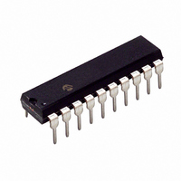
IC PIC MCU FLASH 256KX8 20-PDIP
Manufacturer
Microchip Technology
Series
PIC® XLP™ 18Fr
Datasheets
1.PIC18LF13K22-ISS.pdf
(388 pages)
2.PIC18LF13K22-ISS.pdf
(12 pages)
3.PIC18LF13K22-ISS.pdf
(36 pages)
4.PIC18LF14K22-IP.pdf
(382 pages)
Specifications of PIC18LF13K22-I/P
Program Memory Type
FLASH
Program Memory Size
8KB (4K x 16)
Package / Case
20-DIP (0.300", 7.62mm)
Core Processor
PIC
Core Size
8-Bit
Speed
64MHz
Connectivity
I²C, LIN, SPI, UART/USART
Peripherals
Brown-out Detect/Reset, POR, PWM, WDT
Number Of I /o
17
Eeprom Size
256 x 8
Ram Size
256 x 8
Voltage - Supply (vcc/vdd)
1.8 V ~ 3.6 V
Data Converters
A/D 12x10b
Oscillator Type
Internal
Operating Temperature
-40°C ~ 85°C
Processor Series
PIC18LF
Core
PIC
Data Bus Width
8 bit
Data Ram Size
256 B
Interface Type
I2C, MSSP, SPI, USART
Maximum Clock Frequency
32 KHz
Number Of Programmable I/os
18
Number Of Timers
4
Operating Supply Voltage
1.8 V to 3.6 V
Maximum Operating Temperature
+ 125 C
Mounting Style
Through Hole
3rd Party Development Tools
52715-96, 52716-328, 52717-734, 52712-325, EWPIC18
Development Tools By Supplier
PG164130, DV164035, DV244005, DV164005
Minimum Operating Temperature
- 40 C
On-chip Adc
10 bit, 12 Channel
Lead Free Status / RoHS Status
Lead free / RoHS Compliant
Lead Free Status / RoHS Status
Lead free / RoHS Compliant, Lead free / RoHS Compliant


19.0
The module consists of a single SR latch with multiple
Set and Reset inputs as well as selectable latch output.
The SR latch module includes the following features:
• Programmable input selection
• SR latch output is available internally/externally
• Selectable Q and Q output
• Firmware Set and Reset
19.1
The latch is a Set-Reset latch that does not depend on a
clock source. Each of the Set and Reset inputs are
active-high. The latch can be Set or Reset by CxOUT,
INT1 pin, or variable clock. Additionally the SRPS and
the SRPR bits of the SRCON0 register may be used to
Set or Reset the SR latch, respectively. The latch is
reset-dominant, therefore, if both Set and Reset inputs
are high the latch will go to the Reset state. Both the
SRPS and SRPR bits are self resetting which means
that a single write to either of the bits is all that is
necessary to complete a latch Set or Reset operation.
FIGURE 19-1:
2010 Microchip Technology Inc.
Note 1:
SR LATCH
Latch Operation
INT1
INT1
SYNCC2OUT
SYNCC1OUT
SYNCC2OUT
SYNCC1OUT
2:
3:
4:
SRPS
SRPR
SRRCKE
SRSCKE
If R = 1 and S = 1 simultaneously, Q = 0, Q = 1
Pulse generator causes a 2 Q-state pulse width.
Output shown for reference only. See I/O port pin block diagram for more detail.
Name denotes the source of connection at the comparator output.
SRRC1E
SRSC1E
SRRC2E
SRSC2E
SRRPE
SRSPE
SRCLK
SRCLK
SR LATCH SIMPLIFIED BLOCK DIAGRAM
(4)
(4)
(4)
(4)
Gen
Gen
Pulse
Pulse
(2)
(2)
Preliminary
PIC18F1XK22/LF1XK22
SR
Latch
S
R
19.2
The SRQEN and SRNQEN bits of the SRCON0
register control the latch output selection. Both of the
SR latch’s outputs may be directly output to an
independent I/O pin. Control is determined by the state
of bits SRQEN and SRNQEN in registers SRCON0.
The applicable TRIS bit of the corresponding port must
be cleared to enable the port pin output driver.
19.3
Upon any device Reset, the SR latch is not initialized.
The user’s firmware is responsible to initialize the latch
output before enabling it to the output pins.
Q
Q
(1)
Latch Output
Effects of a Reset
SRLEN
SRQEN
SRLEN
SRNQEN
SRQ pin
DS41365D-page 239
SRNQ pin
(3)
(3)
Related parts for PIC18LF13K22-I/P
Image
Part Number
Description
Manufacturer
Datasheet
Request
R

Part Number:
Description:
Manufacturer:
Microchip Technology Inc.
Datasheet:
Part Number:
Description:
Manufacturer:
Microchip Technology Inc.
Datasheet:
Part Number:
Description:
Manufacturer:
Microchip Technology Inc.
Datasheet:
Part Number:
Description:
Manufacturer:
Microchip Technology Inc.
Datasheet:
Part Number:
Description:
Manufacturer:
Microchip Technology Inc.
Datasheet:
Part Number:
Description:
Manufacturer:
Microchip Technology Inc.
Datasheet:
Part Number:
Description:
Manufacturer:
Microchip Technology Inc.
Datasheet:
Part Number:
Description:
Manufacturer:
Microchip Technology Inc.
Datasheet: