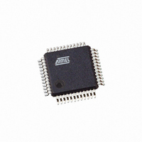
AT91SAM7S32B-AU Atmel, AT91SAM7S32B-AU Datasheet - Page 14

AT91SAM7S32B-AU
Manufacturer Part Number
AT91SAM7S32B-AU
Description
IC MCU ARM7 32KB FLASH 48LQFP
Manufacturer
Atmel
Series
AT91SAMr
Datasheet
1.AT91SAM7S16-MU.pdf
(779 pages)
Specifications of AT91SAM7S32B-AU
Core Processor
ARM7
Core Size
16/32-Bit
Speed
55MHz
Connectivity
I²C, SPI, SSC, UART/USART
Peripherals
Brown-out Detect/Reset, DMA, POR, PWM, WDT
Number Of I /o
21
Program Memory Size
32KB (32K x 8)
Program Memory Type
FLASH
Ram Size
8K x 8
Voltage - Supply (vcc/vdd)
1.65 V ~ 1.95 V
Data Converters
A/D 8x10b
Oscillator Type
Internal
Operating Temperature
-40°C ~ 85°C
Package / Case
48-LQFP
Cpu Family
91S
Device Core
ARM7TDMI
Device Core Size
32b
Frequency (max)
55MHz
Interface Type
SPI/TWI/USART
Total Internal Ram Size
8KB
# I/os (max)
21
Number Of Timers - General Purpose
3
Operating Supply Voltage (typ)
1.8/3.3V
Operating Supply Voltage (max)
1.95/3.6V
Operating Supply Voltage (min)
1.65/3V
On-chip Adc
8-chx10-bit
Instruction Set Architecture
RISC
Operating Temp Range
-40C to 85C
Operating Temperature Classification
Industrial
Mounting
Surface Mount
Pin Count
48
Package Type
LQFP
Package
48LQFP
Family Name
AT91
Maximum Speed
55 MHz
Operating Supply Voltage
1.8|3.3 V
Data Bus Width
32 Bit
Number Of Programmable I/os
21
Number Of Timers
3
For Use With
AT91SAM-ICE - EMULATOR FOR AT91 ARM7/ARM9AT91SAM7S-EK - KIT EVAL FOR ARM AT91SAM7S
Lead Free Status / RoHS Status
Lead free / RoHS Compliant
Eeprom Size
-
Lead Free Status / Rohs Status
Compliant
Available stocks
Company
Part Number
Manufacturer
Quantity
Price
Part Number:
AT91SAM7S32B-AU
Manufacturer:
MICROCHIP/微芯
Quantity:
20 000
- Current page: 14 of 779
- Download datasheet (11Mb)
6. I/O Lines Considerations
6.1
6.2
6.3
6.4
6.5
14
JTAG Port Pins
Test Pin
Reset Pin
ERASE Pin
PIO Controller A Lines
AT91SAM7S Series Preliminary
TMS, TDI and TCK are schmitt trigger inputs. TMS and TCK are 5-V tolerant, TDI is not. TMS,
TDI and TCK do not integrate a pull-up resistor.
TDO is an output, driven at up to VDDIO, and has no pull-up resistor.
The JTAGSEL pin is used to select the JTAG boundary scan when asserted at a high level. The
JTAGSEL pin integrates a permanent pull-down resistor of about 15 kΩ to GND, so that it can be
left unconnected for normal operations.
The TST pin is used for manufacturing test, fast programming mode or SAM-BA Boot Recovery
of the AT91SAM7S Series when asserted high. The TST pin integrates a permanent pull-down
resistor of about 15 kΩ to GND, so that it can be left unconnected for normal operations.
To enter fast programming mode, the TST pin and the PA0 and PA1 pins should be tied high
and PA2 tied to low.
To enter SAM-BA Boot Recovery, the TST pin and the PA0, PA1 and PA2 pins should be tied
high for at least 10 seconds. Then a power cycle of the board is mandatory.
Driving the TST pin at a high level while PA0 or PA1 is driven at 0 leads to unpredictable results.
The NRST pin is bidirectional with an open drain output buffer. It is handled by the on-chip reset
controller and can be driven low to provide a reset signal to the external components or asserted
low externally to reset the microcontroller. There is no constraint on the length of the reset pulse,
and the reset controller can guarantee a minimum pulse length. This allows connection of a sim-
ple push-button on the pin NRST as system user reset, and the use of the signal NRST to reset
all the components of the system.
The NRST pin integrates a permanent pull-up resistor to VDDIO.
The ERASE pin is used to re-initialize the Flash content and some of its NVM bits. It integrates a
permanent pull-down resistor of about 15 kΩ to GND, so that it can be left unconnected for nor-
mal operations.
Programming of this pull-up resistor is performed independently for each I/O line through the
PIO controllers.
5V-tolerant means that the I/O lines can drive voltage level according to VDDIO, but can be
driven with a voltage of up to 5.5V. However, driving an I/O line with a voltage over VDDIO while
the programmable pull-up resistor is enabled will create a current path through the pull-up resis-
• All the I/O lines PA0 to PA31on AT91SAM7S512/256/128/64/321 (PA0 to PA20 on
• All the I/O lines PA0 to PA31 on AT91SAM7S161 (PA0 to PA20 on AT91SAM7S16) are not
AT91SAM7S32) are 5V-tolerant and all integrate a programmable pull-up resistor.
5V-tolerant and all integrate a programmable pull-up resistor.
6175K–ATARM–30-Aug-10
Related parts for AT91SAM7S32B-AU
Image
Part Number
Description
Manufacturer
Datasheet
Request
R

Part Number:
Description:
KIT EVAL FOR ARM AT91SAM7S
Manufacturer:
Atmel
Datasheet:

Part Number:
Description:
MCU, MPU & DSP Development Tools KICKSTART KIT ATMEL AT91SAM7S
Manufacturer:
IAR Systems

Part Number:
Description:
DEV KIT FOR AVR/AVR32
Manufacturer:
Atmel
Datasheet:

Part Number:
Description:
INTERVAL AND WIPE/WASH WIPER CONTROL IC WITH DELAY
Manufacturer:
ATMEL Corporation
Datasheet:

Part Number:
Description:
Low-Voltage Voice-Switched IC for Hands-Free Operation
Manufacturer:
ATMEL Corporation
Datasheet:

Part Number:
Description:
MONOLITHIC INTEGRATED FEATUREPHONE CIRCUIT
Manufacturer:
ATMEL Corporation
Datasheet:

Part Number:
Description:
AM-FM Receiver IC U4255BM-M
Manufacturer:
ATMEL Corporation
Datasheet:

Part Number:
Description:
Monolithic Integrated Feature Phone Circuit
Manufacturer:
ATMEL Corporation
Datasheet:

Part Number:
Description:
Multistandard Video-IF and Quasi Parallel Sound Processing
Manufacturer:
ATMEL Corporation
Datasheet:

Part Number:
Description:
High-performance EE PLD
Manufacturer:
ATMEL Corporation
Datasheet:

Part Number:
Description:
8-bit Flash Microcontroller
Manufacturer:
ATMEL Corporation
Datasheet:

Part Number:
Description:
2-Wire Serial EEPROM
Manufacturer:
ATMEL Corporation
Datasheet:


