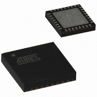
AT89C5130A-PUTUM Atmel, AT89C5130A-PUTUM Datasheet - Page 95

AT89C5130A-PUTUM
Manufacturer Part Number
AT89C5130A-PUTUM
Description
IC 8051 MCU FLASH 16K USB 32QFN
Manufacturer
Atmel
Series
AT89C513xr
Datasheet
1.AT89C5130A-PUTUM.pdf
(188 pages)
Specifications of AT89C5130A-PUTUM
Core Processor
C52X2
Core Size
8-Bit
Speed
48MHz
Connectivity
I²C, SPI, UART/USART, USB
Peripherals
LED, POR, PWM, WDT
Number Of I /o
18
Program Memory Size
16KB (16K x 8)
Program Memory Type
FLASH
Eeprom Size
4K x 8
Ram Size
1.25K x 8
Voltage - Supply (vcc/vdd)
2.7 V ~ 5.5 V
Oscillator Type
Internal
Operating Temperature
-40°C ~ 85°C
Package / Case
32-VQFN Exposed Pad, 32-HVQFN, 32-SQFN, 32-DHVQFN
Package
32QFN EP
Device Core
8051
Family Name
89C
Maximum Speed
48 MHz
Operating Supply Voltage
3.3|5 V
Data Bus Width
8 Bit
Number Of Programmable I/os
34
Interface Type
SPI/TWI/UART/USB
Number Of Timers
3
Processor Series
AT89x
Core
8051
Data Ram Size
1.25 KB
Maximum Clock Frequency
48 MHz
Maximum Operating Temperature
+ 85 C
Mounting Style
SMD/SMT
3rd Party Development Tools
PK51, CA51, A51, ULINK2
Development Tools By Supplier
AT89STK-05
Minimum Operating Temperature
- 40 C
Height
0.95 mm
Length
7 mm
Supply Voltage (max)
5.5 V
Supply Voltage (min)
2.7 V
Width
7 mm
For Use With
AT89OCD-01 - USB EMULATOR FOR AT8XC51 MCU
Lead Free Status / RoHS Status
Lead free / RoHS Compliant
Data Converters
-
Lead Free Status / Rohs Status
Details
Other names
AT89C5130A-PUTIM
AT89C5130A-PUTIM
AT89C5130A-PUTIM
Available stocks
Company
Part Number
Manufacturer
Quantity
Price
Company:
Part Number:
AT89C5130A-PUTUM
Manufacturer:
Atmel
Quantity:
5
19.3
19.3.1
4337K–USB–04/08
Functional Description
Operating Modes
Figure 19-2
Figure 19-2. SPI Module Block Diagram
The Serial Peripheral Interface can be configured as one of the two modes: Master mode or
Slave mode. The configuration and initialization of the SPI module is made through one register:
Once the SPI is configured, the data exchange is made using:
During an SPI transmission, data is simultaneously transmitted (shifted out serially) and
received (shifted in serially). A serial clock line (SCK) synchronizes shifting and sampling on the
two serial data lines (MOSI and MISO). A Slave Select line (SS) allows individual selection of a
Slave SPI device; Slave devices that are not selected do not interfere with SPI bus activities.
• The Serial Peripheral CONtrol register (SPCON)
• SPCON
• The Serial Peripheral STAtus register (SPSTA)
• The Serial Peripheral DATa register (SPDAT)
SPR2
1
SPI Interrupt Request
shows a detailed structure of the SPI module.
SPR1
1
Clock
Divider
SPR0
FCLK PERIPH
SPR2
1
/128
/16
/32
/64
SPEN
/8
/4
Clock
Select
SSDIS
MSTR
SPIF
Clock Rate
Don’t Use
Receive Data Register
CPOL
WCOL
7
Shift Register
Internal Bus
6
SPI
Control
CPHA
5
SSERR
4
3
AT89C5130A/31A-M
SPR1
2
Clock
Logic
SPCON
1
SPDAT
MODF
0
SPR0
-
Baud Rate Divisor (BD)
M
Pin
Control
Logic
S
-
No BRG
-
SPSTA
-
8-bit bus
1-bit signal
MOSI
MISO
SCK
SS
95


