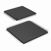
DSPIC33FJ32GS610-I/PT Microchip Technology, DSPIC33FJ32GS610-I/PT Datasheet - Page 219

DSPIC33FJ32GS610-I/PT
Manufacturer Part Number
DSPIC33FJ32GS610-I/PT
Description
IC MCU/DSP 32KB FLASH 100TQFP
Manufacturer
Microchip Technology
Series
dsPIC™ 33Fr
Specifications of DSPIC33FJ32GS610-I/PT
Core Processor
dsPIC
Core Size
16-Bit
Speed
40 MIPs
Connectivity
I²C, IrDA, LIN, SPI, UART/USART
Peripherals
Brown-out Detect/Reset, QEI, POR, PWM, WDT
Number Of I /o
85
Program Memory Size
32KB (32K x 8)
Program Memory Type
FLASH
Ram Size
4K x 8
Voltage - Supply (vcc/vdd)
3 V ~ 3.6 V
Data Converters
A/D 24x10b, D/A 1x10b
Oscillator Type
Internal
Operating Temperature
-40°C ~ 85°C
Package / Case
100-TFQFP
Core Frequency
40MHz
Embedded Interface Type
I2C, SPI, UART
No. Of I/o's
85
Flash Memory Size
32KB
Supply Voltage Range
3V To 3.6V
Rohs Compliant
Yes
Lead Free Status / RoHS Status
Lead free / RoHS Compliant
Eeprom Size
-
Lead Free Status / RoHS Status
Lead free / RoHS Compliant, Lead free / RoHS Compliant
Available stocks
Company
Part Number
Manufacturer
Quantity
Price
Company:
Part Number:
DSPIC33FJ32GS610-I/PT
Manufacturer:
Microchip
Quantity:
387
Company:
Part Number:
DSPIC33FJ32GS610-I/PT
Manufacturer:
Microchip Technology
Quantity:
10 000
Part Number:
DSPIC33FJ32GS610-I/PT
Manufacturer:
MICROCHIP/微芯
Quantity:
20 000
- Current page: 219 of 418
- Download datasheet (3Mb)
14.0
The input capture module is useful in applications
requiring frequency (period) and pulse measurement.
The
dsPIC33FJ64GS406/606/608/610 devices support up to
two input capture channels.
The input capture module captures the 16-bit value of
the selected Time Base register when an event occurs
at the ICx pin. The events that cause a capture event
are listed below in three categories:
FIGURE 14-1:
2010 Microchip Technology Inc.
dsPIC33FJ32GS406/606/608/610 and dsPIC33FJ64GS406/606/608/610
Note 1: This data sheet summarizes the features
ICx Pin
Note 1: An ‘x’ in a signal, register or bit name denotes the number of the capture channel.
2: Some registers and associated bits
INPUT CAPTURE
dsPIC33FJ32GS406/606/608/610
of the dsPIC33FJ32GS406/606/608/610
and
families of devices. It is not intended to be
a comprehensive reference source. To
complement the information in this data
sheet, refer to Section 12. “Input Cap-
ture” (DS70198) in the “dsPIC33F/
PIC24H
which is available from the Microchip web
site (www.microchip.com).
described in this section may not be avail-
able on all devices. Refer to Section 4.0
“Memory Organization” in this data
sheet for device-specific register and bit
information.
Prescaler
(1, 4, 16)
Counter
dsPIC33FJ64GS406/606/608/610
3
INPUT CAPTURE BLOCK DIAGRAM
Family
System Bus
ICxCON
ICM<2:0> (ICxCON<2:0>)
ICOV, ICBNE (ICxCON<4:3>)
Mode Select
Reference
Edge Detection Logic
Clock Synchronizer
ICxI<1:0>
Manual”,
and
and
Preliminary
(in IFSx Register)
Set Flag ICxIF
Interrupt
Logic
• Simple Capture Event modes:
• Capture timer value on every edge (rising and
• Prescaler Capture Event modes:
Each input capture channel can select one of the
two 16-bit timers (Timer2 or Timer3) for the time
base. The selected timer can use either an internal
or external clock.
Other operational features include:
• Device wake-up from capture pin during CPU
• Interrupt on input capture event
• 4-word FIFO buffer for capture values
• Use of input capture to provide additional sources
- Capture timer value on every falling edge of
- Capture timer value on every rising edge of
falling)
- Capture timer value on every 4th rising edge
- Capture timer value on every 16th rising
Sleep and Idle modes
- Interrupt optionally generated after 1, 2, 3 or
of external interrupts
input at ICx pin
input at ICx pin
of input at ICx pin
edge of input at ICx pin
4 buffer locations are filled
Logic
FIFO
R/W
From 16-Bit Timers
TMR2 TMR3
1
ICxBUF
16
0
DS70591C-page 219
16
ICTMR
(ICxCON<7>)
Related parts for DSPIC33FJ32GS610-I/PT
Image
Part Number
Description
Manufacturer
Datasheet
Request
R

Part Number:
Description:
IC, DSC, 16BIT, 12KB, 40MHZ, 3.6V, DIP28
Manufacturer:
Microchip Technology
Datasheet:

Part Number:
Description:
Manufacturer:
Microchip Technology Inc.
Datasheet:

Part Number:
Description:
Manufacturer:
Microchip Technology Inc.
Datasheet:

Part Number:
Description:
Manufacturer:
Microchip Technology Inc.
Datasheet:

Part Number:
Description:
Manufacturer:
Microchip Technology Inc.
Datasheet:

Part Number:
Description:
Manufacturer:
Microchip Technology Inc.
Datasheet:

Part Number:
Description:
Manufacturer:
Microchip Technology Inc.
Datasheet:

Part Number:
Description:
Manufacturer:
Microchip Technology Inc.
Datasheet:

Part Number:
Description:
Manufacturer:
Microchip Technology Inc.
Datasheet:


