DSPIC33FJ32GS610-I/PT Microchip Technology, DSPIC33FJ32GS610-I/PT Datasheet - Page 231
DSPIC33FJ32GS610-I/PT
Manufacturer Part Number
DSPIC33FJ32GS610-I/PT
Description
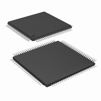
IC MCU/DSP 32KB FLASH 100TQFP
Manufacturer
Microchip Technology
Series
dsPIC™ 33Fr
Specifications of DSPIC33FJ32GS610-I/PT
Core Processor
dsPIC
Core Size
16-Bit
Speed
40 MIPs
Connectivity
I²C, IrDA, LIN, SPI, UART/USART
Peripherals
Brown-out Detect/Reset, QEI, POR, PWM, WDT
Number Of I /o
85
Program Memory Size
32KB (32K x 8)
Program Memory Type
FLASH
Ram Size
4K x 8
Voltage - Supply (vcc/vdd)
3 V ~ 3.6 V
Data Converters
A/D 24x10b, D/A 1x10b
Oscillator Type
Internal
Operating Temperature
-40°C ~ 85°C
Package / Case
100-TFQFP
Core Frequency
40MHz
Embedded Interface Type
I2C, SPI, UART
No. Of I/o's
85
Flash Memory Size
32KB
Supply Voltage Range
3V To 3.6V
Rohs Compliant
Yes
Lead Free Status / RoHS Status
Lead free / RoHS Compliant
Eeprom Size
-
Lead Free Status / RoHS Status
Lead free / RoHS Compliant, Lead free / RoHS Compliant
Available stocks
Company
Part Number
Manufacturer
Quantity
Price
Company:

Part Number:
DSPIC33FJ32GS610-I/PT
Manufacturer:
Microchip
Quantity:
387
Company:
Part Number:
DSPIC33FJ32GS610-I/PT
Manufacturer:
Microchip Technology
Quantity:
10 000
Part Number:
DSPIC33FJ32GS610-I/PT
Manufacturer:
MICROCHIP/微芯
Quantity:
20 000


REGISTER 16-2:
REGISTER 16-3:
2010 Microchip Technology Inc.
bit 15
bit 7
Legend:
R = Readable bit
-n = Value at POR
bit 15-3
bit 2-0
bit 15
bit 7
Legend:
R = Readable bit
-n = Value at POR
bit 15-0
dsPIC33FJ32GS406/606/608/610 and dsPIC33FJ64GS406/606/608/610
Note 1: These bits should be changed only when PTEN = 0. Changing the clock selection during operation will
Note 1: The PWM time base has a minimum value of 0x0010, and a maximum value of 0xFFF8.
R/W-1
R/W-1
U-0
U-0
—
—
2: Any Period value that is less than 0x0028 must have the least significant 3 bits set to ‘0’, thus yielding a
yield unpredictable results.
Period resolution at 8.32 ns (at fastest auxiliary clock rate).
Unimplemented: Read as ‘0’
PCLKDIV<2:0>: PWM Input Clock Prescaler (Divider) Select bits
111 = Reserved
110 = Divide by 64, maximum PWM timing resolution
101 = Divide by 32, maximum PWM timing resolution
100 = Divide by 16, maximum PWM timing resolution
011 = Divide by 8, maximum PWM timing resolution
010 = Divide by 4, maximum PWM timing resolution
001 = Divide by 2, maximum PWM timing resolution
000 = Divide by 1, maximum PWM timing resolution (power-on default)
PTPER<15:0>: Primary Master Time Base (PMTMR) Period Value bits
R/W-1
R/W-1
U-0
U-0
—
—
PTCON2: PWM CLOCK DIVIDER SELECT REGISTER
PTPER: PRIMARY MASTER TIME BASE PERIOD REGISTER
W = Writable bit
‘1’ = Bit is set
W = Writable bit
‘1’ = Bit is set
R/W-1
R/W-1
U-0
U-0
—
—
R/W-1
R/W-1
U-0
U-0
Preliminary
—
—
PTPER<15:8>
PTPER<7:0>
U = Unimplemented bit, read as ‘0’
U = Unimplemented bit, read as ‘0’
‘0’ = Bit is cleared
‘0’ = Bit is cleared
R/W-1
R/W-1
U-0
U-0
—
—
R/W-0
R/W-1
R/W-0
U-0
—
(1)
PCLKDIV<2:0>
x = Bit is unknown
x = Bit is unknown
R/W-0
R/W-1
R/W-0
(1,2)
U-0
—
DS70591C-page 231
(1)
R/W-0
R/W-1
R/W-0
U-0
—
bit 8
bit 0
bit 8
bit 0
Related parts for DSPIC33FJ32GS610-I/PT
Image
Part Number
Description
Manufacturer
Datasheet
Request
R

Part Number:
Description:
IC, DSC, 16BIT, 12KB, 40MHZ, 3.6V, DIP28
Manufacturer:
Microchip Technology
Datasheet:

Part Number:
Description:
Manufacturer:
Microchip Technology Inc.
Datasheet:
Part Number:
Description:
Manufacturer:
Microchip Technology Inc.
Datasheet:
Part Number:
Description:
Manufacturer:
Microchip Technology Inc.
Datasheet:
Part Number:
Description:
Manufacturer:
Microchip Technology Inc.
Datasheet:
Part Number:
Description:
Manufacturer:
Microchip Technology Inc.
Datasheet:
Part Number:
Description:
Manufacturer:
Microchip Technology Inc.
Datasheet:
Part Number:
Description:
Manufacturer:
Microchip Technology Inc.
Datasheet:
Part Number:
Description:
Manufacturer:
Microchip Technology Inc.
Datasheet: