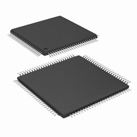
DSPIC33FJ32GS610-I/PT Microchip Technology, DSPIC33FJ32GS610-I/PT Datasheet - Page 305

DSPIC33FJ32GS610-I/PT
Manufacturer Part Number
DSPIC33FJ32GS610-I/PT
Description
IC MCU/DSP 32KB FLASH 100TQFP
Manufacturer
Microchip Technology
Series
dsPIC™ 33Fr
Specifications of DSPIC33FJ32GS610-I/PT
Core Processor
dsPIC
Core Size
16-Bit
Speed
40 MIPs
Connectivity
I²C, IrDA, LIN, SPI, UART/USART
Peripherals
Brown-out Detect/Reset, QEI, POR, PWM, WDT
Number Of I /o
85
Program Memory Size
32KB (32K x 8)
Program Memory Type
FLASH
Ram Size
4K x 8
Voltage - Supply (vcc/vdd)
3 V ~ 3.6 V
Data Converters
A/D 24x10b, D/A 1x10b
Oscillator Type
Internal
Operating Temperature
-40°C ~ 85°C
Package / Case
100-TFQFP
Core Frequency
40MHz
Embedded Interface Type
I2C, SPI, UART
No. Of I/o's
85
Flash Memory Size
32KB
Supply Voltage Range
3V To 3.6V
Rohs Compliant
Yes
Lead Free Status / RoHS Status
Lead free / RoHS Compliant
Eeprom Size
-
Lead Free Status / RoHS Status
Lead free / RoHS Compliant, Lead free / RoHS Compliant
Available stocks
Company
Part Number
Manufacturer
Quantity
Price
Company:
Part Number:
DSPIC33FJ32GS610-I/PT
Manufacturer:
Microchip
Quantity:
387
Company:
Part Number:
DSPIC33FJ32GS610-I/PT
Manufacturer:
Microchip Technology
Quantity:
10 000
Part Number:
DSPIC33FJ32GS610-I/PT
Manufacturer:
MICROCHIP/微芯
Quantity:
20 000
- Current page: 305 of 418
- Download datasheet (3Mb)
22.0
The
dsPIC33FJ64GS406/606/608/610
high-speed successive approximation Analog-to-Digital
conversions to support applications such as AC/DC and
DC/DC power converters.
22.1
The ADC module incorporates the following features:
• 10-bit resolution
• Unipolar inputs
• Up to two Successive Approximation Registers
• Up to 24 external input channels
• Two internal analog inputs
• Dedicated result register for each analog input
• ±1 LSB accuracy at 3.3V
• Single supply operation
• 4 Msps conversion rate at 3.3V (devices with two
• 2 Msps conversion rate at 3.3V (devices with one
• Low-power CMOS technology
2010 Microchip Technology Inc.
(SARs)
SARs)
SAR)
dsPIC33FJ32GS406/606/608/610 and dsPIC33FJ64GS406/606/608/610
Note 1: This data sheet summarizes the features
2: Some registers and associated bits
HIGH-SPEED 10-BIT
ANALOG-TO-DIGITAL
CONVERTER (ADC)
Features Overview
dsPIC33FJ32GS406/606/608/610
of the dsPIC33FJ32GS406/606/608/610
and
families of devices. It is not intended to be
a comprehensive reference source. To
complement the information in this data
sheet, refer to Section 44. “High-Speed
10-Bit
(ADC)”
“dsPIC33F/PIC24H Family Reference
Manual”, which is available from the
Microchip web site (www.microchip.com).
described in this section may not be avail-
able on all devices. Refer to Section 4.0
“Memory Organization” in this data
sheet for device-specific register and bit
information.
dsPIC33FJ64GS406/606/608/610
Analog-to-Digital
(DS70321)
devices
in
Converter
provide
the
and
Preliminary
22.2
This ADC module is designed for applications that
require low latency between the request for conversion
and the resultant output data. Typical applications
include:
• AC/DC power supplies
• DC/DC converters
• Power Factor Correction (PFC)
This ADC works with the high-speed PWM module in
power control applications that require high-frequency
control loops. This module can sample and convert two
analog inputs in a 0.5 microsecond when two SARs are
used. This small conversion delay reduces the “phase
lag” between measurement and control system
response.
Up to five inputs may be sampled at a time (four inputs
from the dedicated sample and hold circuits and one
from the shared sample and hold circuit). If multiple
inputs request conversion, the ADC will convert them in
a sequential manner, starting with the lowest order
input.
This ADC design provides each pair of analog inputs
(AN1,AN0), (AN3,AN2),..., the ability to specify its own
trigger source out of a maximum of sixteen different
trigger sources. This capability allows this ADC to
sample and convert analog inputs that are associated
with PWM generators operating on independent time
bases.
The user application typically requires synchronization
between analog data sampling and PWM output to the
application circuit. The very high-speed operation of
this ADC module allows “data on demand”.
In addition, several hardware features have been
added to the peripheral interface to improve real-time
performance in a typical DSP-based application.
• Result alignment options
• Automated sampling
• External conversion start control
• Two internal inputs to monitor 1.2V internal
A block diagram of the ADC module is shown in
Figure 22-2.
reference and EXTREF input signal
Module Description
DS70591C-page 305
Related parts for DSPIC33FJ32GS610-I/PT
Image
Part Number
Description
Manufacturer
Datasheet
Request
R

Part Number:
Description:
IC, DSC, 16BIT, 12KB, 40MHZ, 3.6V, DIP28
Manufacturer:
Microchip Technology
Datasheet:

Part Number:
Description:
Manufacturer:
Microchip Technology Inc.
Datasheet:

Part Number:
Description:
Manufacturer:
Microchip Technology Inc.
Datasheet:

Part Number:
Description:
Manufacturer:
Microchip Technology Inc.
Datasheet:

Part Number:
Description:
Manufacturer:
Microchip Technology Inc.
Datasheet:

Part Number:
Description:
Manufacturer:
Microchip Technology Inc.
Datasheet:

Part Number:
Description:
Manufacturer:
Microchip Technology Inc.
Datasheet:

Part Number:
Description:
Manufacturer:
Microchip Technology Inc.
Datasheet:

Part Number:
Description:
Manufacturer:
Microchip Technology Inc.
Datasheet:


