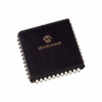
PIC16LF877-04/L Microchip Technology, PIC16LF877-04/L Datasheet - Page 133

PIC16LF877-04/L
Manufacturer Part Number
PIC16LF877-04/L
Description
IC MCU FLASH 8KX14 EE A/D 44PLCC
Manufacturer
Microchip Technology
Series
PIC® 16Fr
Datasheet
1.PIC16F873-04SO.pdf
(218 pages)
Specifications of PIC16LF877-04/L
Core Size
8-Bit
Program Memory Size
14KB (8K x 14)
Core Processor
PIC
Speed
4MHz
Connectivity
I²C, SPI, UART/USART
Peripherals
Brown-out Detect/Reset, POR, PWM, WDT
Number Of I /o
33
Program Memory Type
FLASH
Eeprom Size
256 x 8
Ram Size
368 x 8
Voltage - Supply (vcc/vdd)
2 V ~ 5.5 V
Data Converters
A/D 8x10b
Oscillator Type
External
Operating Temperature
0°C ~ 70°C
Package / Case
44-PLCC
Controller Family/series
PIC16LF
No. Of I/o's
33
Eeprom Memory Size
256Byte
Ram Memory Size
368Byte
Cpu Speed
4MHz
No. Of Timers
3
Lead Free Status / RoHS Status
Lead free / RoHS Compliant
Available stocks
Company
Part Number
Manufacturer
Quantity
Price
Company:
Part Number:
PIC16LF877-04/L
Manufacturer:
Microchip Technology
Quantity:
10 000
- Current page: 133 of 218
- Download datasheet (4Mb)
12.12 Watchdog Timer (WDT)
The Watchdog Timer is a free running on-chip RC oscil-
lator which does not require any external components.
This RC oscillator is separate from the RC oscillator of
the OSC1/CLKIN pin. That means that the WDT will
run, even if the clock on the OSC1/CLKIN and OSC2/
CLKOUT pins of the device has been stopped, for
example, by execution of a SLEEP instruction.
During normal operation, a WDT time-out generates a
device RESET (Watchdog Timer Reset). If the device is
in SLEEP mode, a WDT time-out causes the device to
wake-up and continue with normal operation (Watch-
dog Timer Wake-up). The TO bit in the STATUS regis-
ter will be cleared upon a Watchdog Timer time-out.
The WDT can be permanently disabled by clearing
configuration bit WDTE (Section 12.1).
FIGURE 12-10:
TABLE 12-7:
2007h
81h,181h
Legend: Shaded cells are not used by the Watchdog Timer.
Note 1: See Register 12-1 for operation of these bits.
Address
2001 Microchip Technology Inc.
Note:
Config. bits
PSA and PS2:PS0 are bits in the OPTION_REG register.
OPTION_REG
Name
SUMMARY OF WATCHDOG TIMER REGISTERS
WATCHDOG TIMER BLOCK DIAGRAM
WDT Timer
Enable Bit
WDT
RBPU
From TMR0 Clock Source
(Figure 5-1)
Bit 7
(1)
BODEN
INTEDG
Bit 6
0
1
(1)
PSA
M
U
X
T0CS
Bit 5
CP1
WDT time-out period values may be found in the Elec-
trical Specifications section under parameter #31. Val-
ues for the WDT prescaler (actually a postscaler, but
shared with the Timer0 prescaler) may be assigned
using the OPTION_REG register.
T0SE
Bit 4
CP0
0
Note 1: The CLRWDT and SLEEP instructions
Time-out
8 - to - 1 MUX
MUX
WDT
Postscaler
2: When a CLRWDT instruction is executed
PWRTE
1
clear the WDT and the postscaler, if
assigned to the WDT, and prevent it from
timing out and generating a device
RESET condition.
Bit 3
and the prescaler is assigned to the WDT,
the prescaler count will be cleared, but
the prescaler assignment is not changed.
PSA
8
(1)
PSA
To TMR0 ( Figure 5-1 )
WDTE
Bit 2
PS2
PIC16F87X
PS2:PS0
FOSC1
Bit 1
DS30292C-page 131
PS1
FOSC0
Bit 0
PS0
Related parts for PIC16LF877-04/L
Image
Part Number
Description
Manufacturer
Datasheet
Request
R

Part Number:
Description:
IC MCU FLASH 4KX14 EEPROM 18SOIC
Manufacturer:
Microchip Technology
Datasheet:

Part Number:
Description:
IC MCU FLASH 4KX14 EEPROM 18DIP
Manufacturer:
Microchip Technology
Datasheet:

Part Number:
Description:
IC MCU FLASH 4KX14 EEPROM 20SSOP
Manufacturer:
Microchip Technology
Datasheet:

Part Number:
Description:
(PIC16LF87 / PIC16LF88) 18/20/28-Pin Enhanced FLASH Microcontrollers with nanoWatt Technology
Manufacturer:
Microchip Technology

Part Number:
Description:
IC MCU FLASH 4KX14 EEPROM 28QFN
Manufacturer:
Microchip Technology
Datasheet:

Part Number:
Description:
Manufacturer:
Microchip Technology Inc.
Datasheet:

Part Number:
Description:
Manufacturer:
Microchip Technology Inc.
Datasheet:

Part Number:
Description:
Manufacturer:
Microchip Technology Inc.
Datasheet:

Part Number:
Description:
Manufacturer:
Microchip Technology Inc.
Datasheet:

Part Number:
Description:
Manufacturer:
Microchip Technology Inc.
Datasheet:

Part Number:
Description:
Manufacturer:
Microchip Technology Inc.
Datasheet:


