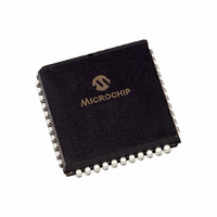
PIC16LF877-04/L Microchip Technology, PIC16LF877-04/L Datasheet - Page 75

PIC16LF877-04/L
Manufacturer Part Number
PIC16LF877-04/L
Description
IC MCU FLASH 8KX14 EE A/D 44PLCC
Manufacturer
Microchip Technology
Series
PIC® 16Fr
Datasheet
1.PIC16F873-04SO.pdf
(218 pages)
Specifications of PIC16LF877-04/L
Core Size
8-Bit
Program Memory Size
14KB (8K x 14)
Core Processor
PIC
Speed
4MHz
Connectivity
I²C, SPI, UART/USART
Peripherals
Brown-out Detect/Reset, POR, PWM, WDT
Number Of I /o
33
Program Memory Type
FLASH
Eeprom Size
256 x 8
Ram Size
368 x 8
Voltage - Supply (vcc/vdd)
2 V ~ 5.5 V
Data Converters
A/D 8x10b
Oscillator Type
External
Operating Temperature
0°C ~ 70°C
Package / Case
44-PLCC
Controller Family/series
PIC16LF
No. Of I/o's
33
Eeprom Memory Size
256Byte
Ram Memory Size
368Byte
Cpu Speed
4MHz
No. Of Timers
3
Lead Free Status / RoHS Status
Lead free / RoHS Compliant
Available stocks
Company
Part Number
Manufacturer
Quantity
Price
Company:
Part Number:
PIC16LF877-04/L
Manufacturer:
Microchip Technology
Quantity:
10 000
- Current page: 75 of 218
- Download datasheet (4Mb)
9.2
The MSSP module in I
master and slave functions (including general call sup-
port) and provides interrupts on START and STOP bits in
hardware, to determine a free bus (multi-master func-
tion). The MSSP module implements the standard mode
specifications, as well as 7-bit and 10-bit addressing.
Refer to Application Note AN578, "Use of the SSP
Module in the I
A "glitch" filter is on the SCL and SDA pins when the pin
is an input. This filter operates in both the 100 kHz and
400 kHz modes. In the 100 kHz mode, when these pins
are an output, there is a slew rate control of the pin that
is independent of device frequency.
FIGURE 9-5:
Two pins are used for data transfer. These are the SCL
pin, which is the clock, and the SDA pin, which is the
data. The SDA and SCL pins are automatically config-
ured when the I
functions are enabled by setting SSP Enable bit
SSPEN (SSPCON<5>).
The MSSP module has six registers for I
They are the:
• SSP Control Register (SSPCON)
• SSP Control Register2 (SSPCON2)
• SSP Status Register (SSPSTAT)
• Serial Receive/Transmit Buffer (SSPBUF)
• SSP Shift Register (SSPSR) - Not directly
• SSP Address Register (SSPADD)
accessible
2001 Microchip Technology Inc.
SDA
SCL
MSSP I
2
2
Read
Clock
C Multi-Master Environment."
Shift
C mode is enabled. The SSP module
2
C Operation
MSb
I
DIAGRAM
STOP bit Detect
2
2
SSPADD Reg
SSPBUF Reg
Match Detect
C SLAVE MODE BLOCK
SSPSR Reg
START and
C mode, fully implements all
LSb
Write
(SSPSTAT Reg)
Data Bus
2
Internal
C operation.
Set, Reset
S, P bits
Addr Match
The SSPCON register allows control of the I
tion. Four mode selection bits (SSPCON<3:0>) allow
one of the following I
• I
• I
• I
• I
Before selecting any I
must be programmed to inputs by setting the appropri-
ate TRIS bits. Selecting an I
SSPEN bit, enables the SCL and SDA pins to be used
as the clock and data lines in I
tors must be provided externally to the SCL and SDA
pins for the proper operation of the I
The CKE bit (SSPSTAT<6:7>) sets the levels of the
SDA and SCL pins in either Master or Slave mode.
When CKE = 1, the levels will conform to the SMBus
specification. When CKE = 0, the levels will conform to
the I
The SSPSTAT register gives the status of the data
transfer. This information includes detection of a
START (S) or STOP (P) bit, specifies if the received
byte was data or address, if the next byte is the com-
pletion of 10-bit address, and if this will be a read or
write data transfer.
SSPBUF is the register to which the transfer data is
written to, or read from. The SSPSR register shifts the
data in or out of the device. In receive operations, the
SSPBUF and SSPSR create a doubled buffered
receiver. This allows reception of the next byte to begin
before reading the last byte of received data. When the
complete byte is received, it is transferred to the
SSPBUF register and flag bit SSPIF is set. If another
complete byte is received before the SSPBUF register
is read, a receiver overflow has occurred and bit
SSPOV (SSPCON<6>) is set and the byte in the
SSPSR is lost.
The SSPADD register holds the slave address. In
10-bit mode, the user needs to write the high byte of the
address (1111 0 A9 A8 0). Following the high byte
address match, the low byte of the address needs to be
loaded (A7:A0).
other mid-range products)
2
2
2
2
C firmware modes (provided for compatibility to
C Slave mode (7-bit address)
C Slave mode (10-bit address)
C Master mode, clock = OSC/4 (SSPADD +1)
2
C specification.
2
C modes to be selected:
2
C mode, the SCL and SDA pins
PIC16F87X
2
2
C mode by setting the
C mode. Pull-up resis-
2
DS30292C-page 73
C module.
2
C opera-
Related parts for PIC16LF877-04/L
Image
Part Number
Description
Manufacturer
Datasheet
Request
R

Part Number:
Description:
IC MCU FLASH 4KX14 EEPROM 18SOIC
Manufacturer:
Microchip Technology
Datasheet:

Part Number:
Description:
IC MCU FLASH 4KX14 EEPROM 18DIP
Manufacturer:
Microchip Technology
Datasheet:

Part Number:
Description:
IC MCU FLASH 4KX14 EEPROM 20SSOP
Manufacturer:
Microchip Technology
Datasheet:

Part Number:
Description:
(PIC16LF87 / PIC16LF88) 18/20/28-Pin Enhanced FLASH Microcontrollers with nanoWatt Technology
Manufacturer:
Microchip Technology

Part Number:
Description:
IC MCU FLASH 4KX14 EEPROM 28QFN
Manufacturer:
Microchip Technology
Datasheet:

Part Number:
Description:
Manufacturer:
Microchip Technology Inc.
Datasheet:

Part Number:
Description:
Manufacturer:
Microchip Technology Inc.
Datasheet:

Part Number:
Description:
Manufacturer:
Microchip Technology Inc.
Datasheet:

Part Number:
Description:
Manufacturer:
Microchip Technology Inc.
Datasheet:

Part Number:
Description:
Manufacturer:
Microchip Technology Inc.
Datasheet:

Part Number:
Description:
Manufacturer:
Microchip Technology Inc.
Datasheet:


