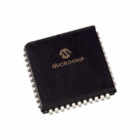
PIC16LF877-04/L Microchip Technology, PIC16LF877-04/L Datasheet - Page 43

PIC16LF877-04/L
Manufacturer Part Number
PIC16LF877-04/L
Description
IC MCU FLASH 8KX14 EE A/D 44PLCC
Manufacturer
Microchip Technology
Series
PIC® 16Fr
Datasheet
1.PIC16F873-04SO.pdf
(218 pages)
Specifications of PIC16LF877-04/L
Core Size
8-Bit
Program Memory Size
14KB (8K x 14)
Core Processor
PIC
Speed
4MHz
Connectivity
I²C, SPI, UART/USART
Peripherals
Brown-out Detect/Reset, POR, PWM, WDT
Number Of I /o
33
Program Memory Type
FLASH
Eeprom Size
256 x 8
Ram Size
368 x 8
Voltage - Supply (vcc/vdd)
2 V ~ 5.5 V
Data Converters
A/D 8x10b
Oscillator Type
External
Operating Temperature
0°C ~ 70°C
Package / Case
44-PLCC
Controller Family/series
PIC16LF
No. Of I/o's
33
Eeprom Memory Size
256Byte
Ram Memory Size
368Byte
Cpu Speed
4MHz
No. Of Timers
3
Lead Free Status / RoHS Status
Lead free / RoHS Compliant
Available stocks
Company
Part Number
Manufacturer
Quantity
Price
Company:
Part Number:
PIC16LF877-04/L
Manufacturer:
Microchip Technology
Quantity:
10 000
4.0
The Data EEPROM and FLASH Program Memory are
readable and writable during normal operation over the
entire V
gle byte for Data EEPROM memory and a single word
for Program memory. A write operation causes an
erase-then-write operation to take place on the speci-
fied byte or word. A bulk erase operation may not be
issued from user code (which includes removing code
protection).
Access to program memory allows for checksum calcu-
lation. The values written to program memory do not
need to be valid instructions. Therefore, up to 14-bit
numbers can be stored in memory for use as calibra-
tion parameters, serial numbers, packed 7-bit ASCII,
etc. Executing a program memory location containing
data that form an invalid instruction, results in the exe-
cution of a NOP instruction.
The EEPROM Data memory is rated for high erase/
write cycles (specification D120). The FLASH program
memory is rated much lower (specification D130),
because EEPROM data memory can be used to store
frequently updated values. An on-chip timer controls
the write time and it will vary with voltage and tempera-
ture, as well as from chip to chip. Please refer to the
specifications for exact limits (specifications D122 and
D133).
A byte or word write automatically erases the location
and writes the new value (erase before write). Writing
to EEPROM data memory does not impact the opera-
tion of the device. Writing to program memory will
cease the execution of instructions until the write is
complete. The program memory cannot be accessed
during the write. During the write operation, the oscilla-
tor continues to run, the peripherals continue to func-
tion and interrupt events will be detected and
essentially “queued” until the write is complete. When
the write completes, the next instruction in the pipeline
is executed and the branch to the interrupt vector will
take place, if the interrupt is enabled and occurred dur-
ing the write.
Read and write access to both memories take place
indirectly through a set of Special Function Registers
(SFR). The six SFRs used are:
• EEDATA
• EEDATH
• EEADR
• EEADRH
• EECON1
• EECON2
2001 Microchip Technology Inc.
DD
DATA EEPROM AND FLASH
PROGRAM MEMORY
range. These operations take place on a sin-
The EEPROM data memory allows byte read and write
operations without interfering with the normal operation
of the microcontroller. When interfacing to EEPROM
data memory, the EEADR register holds the address to
be accessed. Depending on the operation, the EEDATA
register holds the data to be written, or the data read, at
the address in EEADR. The PIC16F873/874 devices
have 128 bytes of EEPROM data memory and there-
fore, require that the MSb of EEADR remain clear. The
EEPROM data memory on these devices do not wrap
around to 0, i.e., 0x80 in the EEADR does not map to
0x00. The PIC16F876/877 devices have 256 bytes of
EEPROM data memory and therefore, uses all 8-bits of
the EEADR.
The FLASH program memory allows non-intrusive
read access, but write operations cause the device to
stop executing instructions, until the write completes.
When interfacing to the program memory, the
EEADRH:EEADR registers form a two-byte word,
which holds the 13-bit address of the memory location
being
EEDATH:EEDATA holds the 14-bit data for writes, or
reflects the value of program memory after a read oper-
ation. Just as in EEPROM data memory accesses, the
value of the EEADRH:EEADR registers must be within
the valid range of program memory, depending on the
device: 0000h to 1FFFh for the PIC16F873/874, or
0000h to 3FFFh for the PIC16F876/877. Addresses
outside of this range do not wrap around to 0000h (i.e.,
4000h does not map to 0000h on the PIC16F877).
4.1
The EECON1 register is the control register for config-
uring and initiating the access. The EECON2 register is
not a physically implemented register, but is used
exclusively in the memory write sequence to prevent
inadvertent writes.
There are many bits used to control the read and write
operations to EEPROM data and FLASH program
memory. The EEPGD bit determines if the access will
be a program or data memory access. When clear, any
subsequent operations will work on the EEPROM data
memory. When set, all subsequent operations will
operate in the program memory.
Read operations only use one additional bit, RD, which
initiates the read operation from the desired memory
location. Once this bit is set, the value of the desired
memory location will be available in the data registers.
This bit cannot be cleared by firmware. It is automati-
cally cleared at the end of the read operation. For
EEPROM data memory reads, the data will be avail-
able in the EEDATA register in the very next instruction
cycle after the RD bit is set. For program memory
reads,
EEDATH:EEDATA registers, following the second
instruction after the RD bit is set.
accessed.
EECON1 and EECON2 Registers
the
data
The
will
PIC16F87X
register
be
loaded
DS30292C-page 41
combination
into
the
of


