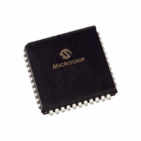
PIC16LF877-04/L Microchip Technology, PIC16LF877-04/L Datasheet - Page 31

PIC16LF877-04/L
Manufacturer Part Number
PIC16LF877-04/L
Description
IC MCU FLASH 8KX14 EE A/D 44PLCC
Manufacturer
Microchip Technology
Series
PIC® 16Fr
Datasheet
1.PIC16F873-04SO.pdf
(218 pages)
Specifications of PIC16LF877-04/L
Core Size
8-Bit
Program Memory Size
14KB (8K x 14)
Core Processor
PIC
Speed
4MHz
Connectivity
I²C, SPI, UART/USART
Peripherals
Brown-out Detect/Reset, POR, PWM, WDT
Number Of I /o
33
Program Memory Type
FLASH
Eeprom Size
256 x 8
Ram Size
368 x 8
Voltage - Supply (vcc/vdd)
2 V ~ 5.5 V
Data Converters
A/D 8x10b
Oscillator Type
External
Operating Temperature
0°C ~ 70°C
Package / Case
44-PLCC
Controller Family/series
PIC16LF
No. Of I/o's
33
Eeprom Memory Size
256Byte
Ram Memory Size
368Byte
Cpu Speed
4MHz
No. Of Timers
3
Lead Free Status / RoHS Status
Lead free / RoHS Compliant
Available stocks
Company
Part Number
Manufacturer
Quantity
Price
Company:
Part Number:
PIC16LF877-04/L
Manufacturer:
Microchip Technology
Quantity:
10 000
- Current page: 31 of 218
- Download datasheet (4Mb)
3.0
Some pins for these I/O ports are multiplexed with an
alternate function for the peripheral features on the
device. In general, when a peripheral is enabled, that
pin may not be used as a general purpose I/O pin.
Additional information on I/O ports may be found in the
PICmicro™ Mid-Range Reference Manual, (DS33023).
3.1
PORTA is a 6-bit wide, bi-directional port. The corre-
sponding data direction register is TRISA. Setting a
TRISA bit (= 1) will make the corresponding PORTA pin
an input (i.e., put the corresponding output driver in a
Hi-Impedance mode). Clearing a TRISA bit (= 0) will
make the corresponding PORTA pin an output (i.e., put
the contents of the output latch on the selected pin).
Reading the PORTA register reads the status of the
pins, whereas writing to it will write to the port latch. All
write operations are read-modify-write operations.
Therefore, a write to a port implies that the port pins are
read, the value is modified and then written to the port
data latch.
Pin RA4 is multiplexed with the Timer0 module clock
input to become the RA4/T0CKI pin. The RA4/T0CKI
pin is a Schmitt Trigger input and an open drain output.
All other PORTA pins have TTL input levels and full
CMOS output drivers.
Other PORTA pins are multiplexed with analog inputs
and analog V
selected by clearing/setting the control bits in the
ADCON1 register (A/D Control Register1).
The TRISA register controls the direction of the RA
pins, even when they are being used as analog inputs.
The user must ensure the bits in the TRISA register are
maintained set when using them as analog inputs.
EXAMPLE 3-1:
BCF
BCF
CLRF
BSF
MOVLW
MOVWF
MOVLW
MOVWF
Note:
2001 Microchip Technology Inc.
I/O PORTS
PORTA and the TRISA Register
STATUS, RP0
STATUS, RP1
PORTA
STATUS, RP0
0x06
ADCON1
0xCF
TRISA
On a Power-on Reset, these pins are con-
figured as analog inputs and read as '0'.
REF
input. The operation of each pin is
INITIALIZING PORTA
;
; Bank0
; Initialize PORTA by
; clearing output
; data latches
; Select Bank 1
; Configure all pins
; as digital inputs
; Value used to
; initialize data
; direction
; Set RA<3:0> as inputs
; RA<5:4> as outputs
; TRISA<7:6>are always
; read as ’0’.
FIGURE 3-1:
FIGURE 3-2:
To A/D Converter
RD Port
Data
Bus
WR
Port
WR
TRIS
RD
TRIS
Note 1: I/O pins have protection diodes to V
Note 1: I/O pin has protection diodes to V
Data
Bus
WR
TRIS
WR
Port
TRIS
RD
RD Port
TMR0 Clock Input
D
TRIS Latch
D
Data Latch
CK
CK
Data Latch
TRIS Latch
D
D
CK
CK
Q
Q
Q
Q
Q
Q
Q
Q
BLOCK DIAGRAM OF
RA3:RA0 AND RA5 PINS
BLOCK DIAGRAM OF
RA4/T0CKI PIN
PIC16F87X
Q
Q
EN
Schmitt
Trigger
Input
Buffer
Analog
Input
Mode
EN
EN
D
DS30292C-page 29
D
V
N
SS
SS
V
V
N
P
DD
SS
DD
only.
and V
I/O pin
TTL
Input
Buffer
I/O pin
SS
.
(1)
(1)
Related parts for PIC16LF877-04/L
Image
Part Number
Description
Manufacturer
Datasheet
Request
R

Part Number:
Description:
IC MCU FLASH 4KX14 EEPROM 18SOIC
Manufacturer:
Microchip Technology
Datasheet:

Part Number:
Description:
IC MCU FLASH 4KX14 EEPROM 18DIP
Manufacturer:
Microchip Technology
Datasheet:

Part Number:
Description:
IC MCU FLASH 4KX14 EEPROM 20SSOP
Manufacturer:
Microchip Technology
Datasheet:

Part Number:
Description:
(PIC16LF87 / PIC16LF88) 18/20/28-Pin Enhanced FLASH Microcontrollers with nanoWatt Technology
Manufacturer:
Microchip Technology

Part Number:
Description:
IC MCU FLASH 4KX14 EEPROM 28QFN
Manufacturer:
Microchip Technology
Datasheet:

Part Number:
Description:
Manufacturer:
Microchip Technology Inc.
Datasheet:

Part Number:
Description:
Manufacturer:
Microchip Technology Inc.
Datasheet:

Part Number:
Description:
Manufacturer:
Microchip Technology Inc.
Datasheet:

Part Number:
Description:
Manufacturer:
Microchip Technology Inc.
Datasheet:

Part Number:
Description:
Manufacturer:
Microchip Technology Inc.
Datasheet:

Part Number:
Description:
Manufacturer:
Microchip Technology Inc.
Datasheet:


