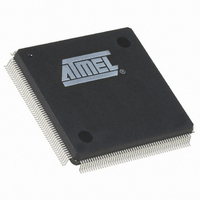
AT91SAM9XE128-QU Atmel, AT91SAM9XE128-QU Datasheet - Page 242

AT91SAM9XE128-QU
Manufacturer Part Number
AT91SAM9XE128-QU
Description
MCU ARM9 128K FLASH 208-PQFP
Manufacturer
Atmel
Series
AT91SAMr
Specifications of AT91SAM9XE128-QU
Core Processor
ARM9
Core Size
16/32-Bit
Speed
180MHz
Connectivity
EBI/EMI, Ethernet, I²C, MMC, SPI, SSC, UART/USART, USB
Peripherals
Brown-out Detect/Reset, POR, PWM, WDT
Number Of I /o
96
Program Memory Size
128KB (128K x 8)
Program Memory Type
FLASH
Ram Size
40K x 8
Voltage - Supply (vcc/vdd)
1.65 V ~ 1.95 V
Data Converters
A/D 4x10b
Oscillator Type
Internal
Operating Temperature
-40°C ~ 85°C
Package / Case
208-MQFP, 208-PQFP
Processor Series
AT91SAMx
Core
ARM926EJ-S
Data Bus Width
32 bit
Data Ram Size
16 KB
Interface Type
2-Wire, EBI, I2S, SPI, USART
Maximum Clock Frequency
180 MHz
Number Of Programmable I/os
96
Number Of Timers
6
Maximum Operating Temperature
+ 85 C
Mounting Style
SMD/SMT
3rd Party Development Tools
JTRACE-ARM-2M, KSK-AT91SAM9XE-PL, MDK-ARM, RL-ARM, ULINK2
Development Tools By Supplier
AT91SAM-ICE, AT91-ISP, AT91SAM9XE-EK
Minimum Operating Temperature
- 40 C
On-chip Adc
10 bit, 4 Channel
For Use With
AT91SAM9XE-EK - KIT EVAL FOR AT91SAM9XEAT91SAM-ICE - EMULATOR FOR AT91 ARM7/ARM9
Lead Free Status / RoHS Status
Lead free / RoHS Compliant
Eeprom Size
-
Lead Free Status / Rohs Status
Lead free / RoHS Compliant
Available stocks
Company
Part Number
Manufacturer
Quantity
Price
- Current page: 242 of 860
- Download datasheet (13Mb)
24.4
24.4.1
6254C–ATARM–22-Jan-10
Product Dependencies
SDRAM Device Initialization
The initialization sequence is generated by software. The SDRAM devices are initialized by the
following sequence:
After initialization, the SDRAM devices are fully functional.
Note:
1. SDRAM features must be set in the configuration register: asynchronous timings (TRC,
2. For mobile SDRAM, temperature-compensated self refresh (TCSR), drive strength
3. The SDRAM memory type must be set in the Memory Device Register.
4. A minimum pause of 200 µs is provided to precede any signal toggle.
5.
6. An All Banks Precharge command is issued to the SDRAM devices. The application
7. Eight auto-refresh (CBR) cycles are provided. The application must set the Mode to 4 in
8. A Mode Register set (MRS) cycle is issued to program the parameters of the SDRAM
9. For mobile SDRAM initialization, an Extended Mode Register set (EMRS) cycle is
10. The application must go into Normal Mode, setting Mode to 0 in the Mode Register and
11. Write the refresh rate into the count field in the SDRAMC Refresh Timer register.
TRAS, etc.), number of columns, rows, CAS latency, and the data bus width.
(DS) and partial array self refresh (PASR) must be set in the Low Power Register.
(1)
1 in the Mode Register and perform a write access to any SDRAM address.
must set Mode to 2 in the Mode Register and perform a write access to any SDRAM
address.
the Mode Register and perform a write access to any SDRAM location eight times.
devices, in particular CAS latency and burst length. The application must set Mode to 3
in the Mode Register and perform a write access to the SDRAM. The write address
must be chosen so that BA[1:0] are set to 0. For example, with a 16-bit 128 MB SDRAM
(12 rows, 9 columns, 4 banks) bank address, the SDRAM write access should be done
at the address 0x20000000.
issued to program the SDRAM parameters (TCSR, PASR, DS). The application must
set Mode to 5 in the Mode Register and perform a write access to the SDRAM. The
write address must be chosen so that BA[1] or BA[0] are set to 1. For example, with a
16-bit 128 MB SDRAM, (12 rows, 9 columns, 4 banks) bank address the SDRAM write
access should be done at the address 0x20800000 or 0x20400000.
performing a write access at any location in the SDRAM.
(Refresh rate = delay between refresh cycles). The SDRAM device requires a refresh
every 15.625 µs or 7.81 µs. With a 100 MHz frequency, the Refresh Timer Counter
Register must be set with the value 1562(15.652 µs x 100 MHz) or 781(7.81 µs x 100
MHz).
A NOP command is issued to the SDRAM devices. The application must set Mode to
1. It is strongly recommended to respect the instructions stated in
cess in order to be certain that the subsequent commands issued by the SDRAMC will be
taken into account.
AT91SAM9XE128/256/512 Preliminary
Step 5
of the initialization pro-
242
Related parts for AT91SAM9XE128-QU
Image
Part Number
Description
Manufacturer
Datasheet
Request
R

Part Number:
Description:
KIT EVAL FOR AT91SAM9XE
Manufacturer:
Atmel
Datasheet:

Part Number:
Description:
MCU ARM9 64K SRAM 144-LFBGA
Manufacturer:
Atmel
Datasheet:

Part Number:
Description:
IC ARM7 MCU FLASH 256K 100LQFP
Manufacturer:
Atmel
Datasheet:

Part Number:
Description:
IC ARM9 MPU 217-LFBGA
Manufacturer:
Atmel
Datasheet:

Part Number:
Description:
MCU ARM9 ULTRA LOW PWR 217-LFBGA
Manufacturer:
Atmel
Datasheet:

Part Number:
Description:
MCU ARM9 324-TFBGA
Manufacturer:
Atmel
Datasheet:

Part Number:
Description:
IC MCU ARM9 SAMPLING 217CBGA
Manufacturer:
Atmel
Datasheet:

Part Number:
Description:
IC ARM9 MCU 217-LFBGA
Manufacturer:
Atmel
Datasheet:

Part Number:
Description:
IC ARM9 MCU 208-PQFP
Manufacturer:
Atmel
Datasheet:

Part Number:
Description:
MCU ARM 512K HS FLASH 100-LQFP
Manufacturer:
Atmel
Datasheet:

Part Number:
Description:
MCU ARM 512K HS FLASH 100-TFBGA
Manufacturer:
Atmel
Datasheet:

Part Number:
Description:
IC ARM9 MCU 200 MHZ 324-TFBGA
Manufacturer:
Atmel
Datasheet:

Part Number:
Description:
IC ARM MCU 16BIT 128K 256BGA
Manufacturer:
Atmel
Datasheet:

Part Number:
Description:
IC ARM7 MCU 32BIT 128K 64LQFP
Manufacturer:
Atmel
Datasheet:

Part Number:
Description:
IC ARM7 MCU FLASH 256K 128-LQFP
Manufacturer:
Atmel
Datasheet:


