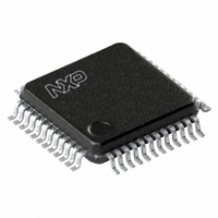
LPC1313FBD48,151 NXP Semiconductors, LPC1313FBD48,151 Datasheet - Page 12

LPC1313FBD48,151
Manufacturer Part Number
LPC1313FBD48,151
Description
IC MCU 32BIT 32KB FLASH 48LQFP
Manufacturer
NXP Semiconductors
Series
LPC13xxr
Specifications of LPC1313FBD48,151
Program Memory Type
FLASH
Program Memory Size
32KB (32K x 8)
Package / Case
48-LQFP
Core Processor
ARM® Cortex-M3™
Core Size
32-Bit
Speed
72MHz
Connectivity
I²C, Microwire, SPI, SSI, UART/USART
Peripherals
Brown-out Detect/Reset, POR, WDT
Number Of I /o
42
Ram Size
8K x 8
Voltage - Supply (vcc/vdd)
2 V ~ 3.6 V
Data Converters
A/D 8x10b
Oscillator Type
Internal
Operating Temperature
-40°C ~ 85°C
Processor Series
LPC13
Core
ARM Cortex M3
Data Bus Width
32 bit
Interface Type
I2C, UART
Maximum Clock Frequency
72 MHz
Number Of Timers
2
Operating Supply Voltage
3.3 V
Maximum Operating Temperature
+ 85 C
Mounting Style
SMD/SMT
3rd Party Development Tools
MDK-ARM, RL-ARM, ULINK2
Development Tools By Supplier
OM11041
Minimum Operating Temperature
- 40 C
On-chip Adc
10 bit, 8 Channel
Cpu Family
LPC1000
Device Core
ARM Cortex-M3
Device Core Size
32b
Frequency (max)
72MHz
Total Internal Ram Size
8KB
# I/os (max)
42
Number Of Timers - General Purpose
4
Operating Supply Voltage (typ)
3.3V
Operating Supply Voltage (max)
3.6V
Operating Supply Voltage (min)
2V
Instruction Set Architecture
RISC
Operating Temp Range
-40C to 85C
Operating Temperature Classification
Industrial
Mounting
Surface Mount
Pin Count
48
Package Type
LQFP
Package
48LQFP
Family Name
LPC1000
Maximum Speed
72 MHz
Number Of Programmable I/os
42
Lead Free Status / RoHS Status
Lead free / RoHS Compliant
For Use With
568-4918 - KIT DEV FOR LPC1313622-1005 - USB IN-CIRCUIT PROG ARM7 LPC2K
Eeprom Size
-
Lead Free Status / Rohs Status
Lead free / RoHS Compliant
Other names
568-4914
935289651151
935289651151
Available stocks
Company
Part Number
Manufacturer
Quantity
Price
Company:
Part Number:
LPC1313FBD48,151
Manufacturer:
MAXIM
Quantity:
1 560
Company:
Part Number:
LPC1313FBD48,151
Manufacturer:
NXP Semiconductors
Quantity:
10 000
NXP Semiconductors
Table 3.
[1]
[2]
[3]
[4]
[5]
[6]
[7]
Table 4.
LPC1311_13_42_43
Product data sheet
Symbol
V
XTALIN
XTALOUT
V
Symbol
RESET/PIO0_0
PIO0_1/CLKOUT/
CT32B0_MAT2/
USB_FTOGGLE
PIO0_2/SSEL/
CT16B0_CAP0
PIO0_3/
USB_VBUS
PIO0_4/SCL
DD
SS
Pin state at reset for default function: I = Input; O = Output; PU = internal pull-up enabled; IA = inactive, no pull-up/down enabled;
F = floating; floating pins, if not used, should be tied to ground or power to minimize power consumption.
See
the chip and wake up from Deep power-down mode.
5 V tolerant pad providing digital I/O functions with configurable pull-up/pull-down resistors and configurable hysteresis (see
I
5 V tolerant pad providing digital I/O functions with configurable pull-up/pull-down resistors, configurable hysteresis, and analog input.
When configured as a ADC input, digital section of the pad is disabled and the pin is not 5 V tolerant (see
Pad provides USB functions. It is designed in accordance with the USB specification, revision 2.0 (Full-speed and Low-speed mode
only).
When the system oscillator is not used, connect XTALIN and XTALOUT as follows: XTALIN can be left floating or can be grounded
(grounding is preferred to reduce susceptibility to noise). XTALOUT should be left floating.
2
C-bus pads compliant with the I
Figure 31
LPC1313/43 LQFP48 pin description table
LPC1311/13/42/43 HVQFN33 pin description table
for pad characteristics. RESET functionality is not available in Deep power-down mode. Use the WAKEUP pin to reset
Pin
2
3
8
9
10
Pin
8;
44
6
7
5;
41
[2]
[3]
[3]
[3]
[7]
[7]
[4]
Start
logic
input
yes
yes
yes
yes
yes
Start
logic
input
-
-
-
-
2
C-bus specification for I
Type Reset
I
I/O
I/O
O
O
O
I/O
I/O
I
I/O
I
I/O
I/O
Type Reset
I
I
O
I
All information provided in this document is subject to legal disclaimers.
state
[1]
I; PU
-
I; PU
-
-
-
I; PU
-
-
I; PU
-
I; IA
-
state
[1]
-
-
-
-
Description
RESET — External reset input: A LOW on this pin resets the device,
causing I/O ports and peripherals to take on their default states, and
processor execution to begin at address 0.
PIO0_0 — General purpose digital input/output pin.
PIO0_1 — General purpose digital input/output pin. A LOW level on this
pin during reset starts the ISP command handler or the USB device
enumeration (USB on LPC1342/43 only, see description of PIO0_3).
CLKOUT — Clock out pin.
CT32B0_MAT2 — Match output 2 for 32-bit timer 0.
USB_FTOGGLE — USB 1 ms Start-of-Frame signal (LPC1342/43 only).
PIO0_2 — General purpose digital input/output pin.
SSEL — Slave select for SSP.
CT16B0_CAP0 — Capture input 0 for 16-bit timer 0.
PIO0_3 — General purpose digital input/output pin. LPC1342/43 only: A
LOW level on this pin during reset starts the ISP command handler, a
HIGH level starts the USB device enumeration.
USB_VBUS — Monitors the presence of USB bus power (LPC1342/43
only).
PIO0_4 — General purpose digital input/output pin (open-drain).
SCL — I
I
Rev. 3 — 10 August 2010
2
C Fast-mode Plus is selected in the I/O configuration register.
Description
3.3 V supply voltage to the internal regulator, the external rail, and the
ADC. Also used as the ADC reference voltage.
Input to the oscillator circuit and internal clock generator circuits. Input
voltage must not exceed 1.8 V.
Output from the oscillator amplifier.
Ground.
2
C standard mode and I
…continued
2
C-bus clock input/output (open-drain). High-current sink only if
2
C Fast-mode Plus.
32-bit ARM Cortex-M3 microcontroller
LPC1311/13/42/43
Figure
© NXP B.V. 2010. All rights reserved.
30).
Figure
12 of 62
30).


