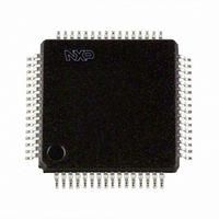
LPC2131FBD64/01,15 NXP Semiconductors, LPC2131FBD64/01,15 Datasheet - Page 9

LPC2131FBD64/01,15
Manufacturer Part Number
LPC2131FBD64/01,15
Description
IC ARM7 MCU FLASH 32K 64-LQFP
Manufacturer
NXP Semiconductors
Series
LPC2100r
Specifications of LPC2131FBD64/01,15
Program Memory Type
FLASH
Program Memory Size
32KB (32K x 8)
Package / Case
64-LQFP
Core Processor
ARM7
Core Size
16/32-Bit
Speed
60MHz
Connectivity
I²C, Microwire, SPI, SSI, SSP, UART/USART
Peripherals
Brown-out Detect/Reset, POR, PWM, WDT
Number Of I /o
47
Ram Size
8K x 8
Voltage - Supply (vcc/vdd)
3 V ~ 3.6 V
Data Converters
A/D 8x10b; D/A 1x10b
Oscillator Type
Internal
Operating Temperature
-40°C ~ 85°C
Processor Series
LPC21
Core
ARM7TDMI-S
Data Bus Width
16 bit, 32 bit
Data Ram Size
8 KB
Interface Type
I2C/SPI/SSP/UART
Maximum Clock Frequency
60 MHz
Number Of Programmable I/os
47
Number Of Timers
2
Operating Supply Voltage
3.3 V
Maximum Operating Temperature
+ 85 C
Mounting Style
SMD/SMT
3rd Party Development Tools
MDK-ARM, RL-ARM, ULINK2
Minimum Operating Temperature
- 40 C
On-chip Adc
8-ch x 10-bit
Cpu Family
LPC2000
Device Core
ARM7TDMI-S
Device Core Size
16/32Bit
Frequency (max)
60MHz
Total Internal Ram Size
8KB
# I/os (max)
47
Number Of Timers - General Purpose
2
Operating Supply Voltage (typ)
3.3V
Operating Supply Voltage (max)
3.6V
Operating Supply Voltage (min)
3V
Instruction Set Architecture
RISC
Operating Temp Range
-40C to 85C
Operating Temperature Classification
Industrial
Mounting
Surface Mount
Pin Count
64
Package Type
LQFP
Package
64LQFP
Family Name
LPC2000
Maximum Speed
60 MHz
Lead Free Status / RoHS Status
Lead free / RoHS Compliant
For Use With
568-4310 - EVAL BOARD LPC2158 W/LCD568-4297 - BOARD EVAL LPC21XX MCB2100MCB2130UME - BOARD EVAL MCB2130 + ULINK-MEMCB2130U - BOARD EVAL MCB2130 + ULINK2MCB2130 - BOARD EVAL NXP LPC213X ARM FAM622-1005 - USB IN-CIRCUIT PROG ARM7 LPC2K568-2095 - BOARD EVAL FOR LPC213X ARM MCU
Eeprom Size
-
Lead Free Status / Rohs Status
Compliant
Other names
568-4005
935281771151
LPC2131FBD64/01-S
935281771151
LPC2131FBD64/01-S
Available stocks
Company
Part Number
Manufacturer
Quantity
Price
Company:
Part Number:
LPC2131FBD64/01,15
Manufacturer:
NXP Semiconductors
Quantity:
10 000
NXP Semiconductors
Table 3.
LPC2131_32_34_36_38
Product data sheet
Symbol
P0.0 to P0.31
P0.0/TXD0/
PWM1
P0.1/RXD0/
PWM3/EINT0
P0.2/SCL0/
CAP0.0
P0.3/SDA0/
MAT0.0/EINT1
P0.4/SCK0/
CAP0.1/AD0.6
P0.5/MISO0/
MAT0.1/AD0.7
P0.6/MOSI0/
CAP0.2/AD1.0
P0.7/SSEL0/
PWM2/EINT2
P0.8/TXD1/
PWM4/AD1.1
P0.9/RXD1/
PWM6/EINT3
P0.10/RTS1/
CAP1.0/AD1.2
Pin description
Pin
19
21
22
26
27
29
30
31
33
34
35
5.2 Pin description
[1]
[2]
[3]
[3]
[4]
[4]
[4]
[2]
[4]
[2]
[4]
Type
I/O
O
O
I
O
I
I/O
I
I/O
O
I
I/O
I
I
I/O
O
I
I/O
I
I
I
O
I
O
O
I
I
O
I
O
I
I
Description
Port 0: Port 0 is a 32-bit I/O port with individual direction controls for each bit. Total of
31 pins of the Port 0 can be used as a general purpose bidirectional digital I/Os while
P0.31 is output only pin. The operation of port 0 pins depends upon the pin function
selected via the pin connect block.
Pin P0.24 is not available.
TXD0 — Transmitter output for UART0.
PWM1 — Pulse Width Modulator output 1.
RXD0 — Receiver input for UART0.
PWM3 — Pulse Width Modulator output 3.
EINT0 — External interrupt 0 input.
SCL0 — I
CAP0.0 — Capture input for Timer 0, channel 0.
SDA0 — I
MAT0.0 — Match output for Timer 0, channel 0.
EINT1 — External interrupt 1 input.
SCK0 — Serial clock for SPI0. SPI clock output from master or input to slave.
CAP0.1 — Capture input for Timer 0, channel 1.
AD0.6 — ADC 0, input 6. This analog input is always connected to its pin.
MISO0 — Master In Slave V
output from SPI slave.
MAT0.1 — Match output for Timer 0, channel 1.
AD0.7 — ADC 0, input 7. This analog input is always connected to its pin.
MOSI0 — Master Out Slave In for SPI0. Data output from SPI master or data input to
SPI slave.
CAP0.2 — Capture input for Timer 0, channel 2.
AD1.0 — ADC 1, input 0. This analog input is always connected to its pin. Available in
LPC2134/36/38 only.
SSEL0 — Slave Select for SPI0. Selects the SPI interface as a slave.
PWM2 — Pulse Width Modulator output 2.
EINT2 — External interrupt 2 input.
TXD1 — Transmitter output for UART1.
PWM4 — Pulse Width Modulator output 4.
AD1.1 — ADC 1, input 1. This analog input is always connected to its pin. Available in
LPC2134/36/38 only.
RXD1 — Receiver input for UART1.
PWM6 — Pulse Width Modulator output 6.
EINT3 — External interrupt 3 input.
RTS1 — Request to Send output for UART1. Available in LPC2134/36/38.
CAP1.0 — Capture input for Timer 1, channel 0.
AD1.2 — ADC 1, input 2. This analog input is always connected to its pin. Available in
LPC2134/36/38 only.
All information provided in this document is subject to legal disclaimers.
2
2
C0 clock input/output. Open drain output (for I
C0 data input/output. Open drain output (for I
Rev. 5 — 2 February 2011
DD
= 3.6 V for SPI0. Data input to SPI master or data
LPC2131/32/34/36/38
Single-chip 16/32-bit microcontrollers
2
2
C-bus compliance).
C-bus compliance).
© NXP B.V. 2011. All rights reserved.
9 of 45


