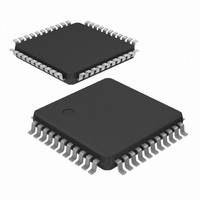
PXAG30KBBD,157 NXP Semiconductors, PXAG30KBBD,157 Datasheet - Page 23

PXAG30KBBD,157
Manufacturer Part Number
PXAG30KBBD,157
Description
IC XA MCU 16BIT ROMLESS 44-LQFP
Manufacturer
NXP Semiconductors
Series
XAr
Datasheet
1.PXAG30KBBD157.pdf
(36 pages)
Specifications of PXAG30KBBD,157
Program Memory Type
ROMless
Package / Case
44-LQFP
Core Processor
XA
Core Size
16-Bit
Speed
30MHz
Connectivity
UART/USART
Peripherals
PWM, WDT
Number Of I /o
32
Ram Size
512 x 8
Voltage - Supply (vcc/vdd)
2.7 V ~ 5.5 V
Oscillator Type
External
Operating Temperature
0°C ~ 70°C
Processor Series
PXAG3x
Core
80C51
Data Bus Width
16 bit
Data Ram Size
512 B
Interface Type
UART
Maximum Clock Frequency
30 MHz
Number Of Programmable I/os
32
Number Of Timers
3
Operating Supply Voltage
2.7 V to 5.5 V
Maximum Operating Temperature
+ 70 C
Mounting Style
SMD/SMT
Minimum Operating Temperature
0 C
Cpu Family
XA
Device Core
80C51
Device Core Size
16b
Frequency (max)
30MHz
Program Memory Size
Not Required
Total Internal Ram Size
512Byte
# I/os (max)
32
Number Of Timers - General Purpose
3
Operating Supply Voltage (typ)
3.3/5V
Operating Supply Voltage (max)
5.5V
Operating Supply Voltage (min)
2.7V
Instruction Set Architecture
CISC
Operating Temp Range
0C to 70C
Operating Temperature Classification
Commercial
Mounting
Surface Mount
Pin Count
44
Package Type
LQFP
Lead Free Status / RoHS Status
Lead free / RoHS Compliant
Eeprom Size
-
Program Memory Size
-
Data Converters
-
Lead Free Status / Rohs Status
Lead free / RoHS Compliant
Other names
568-1300
935270581157
PXAG30KBBD
935270581157
PXAG30KBBD
Available stocks
Company
Part Number
Manufacturer
Quantity
Price
Company:
Part Number:
PXAG30KBBD,157
Manufacturer:
NXP Semiconductors
Quantity:
10 000
1. Ports in Quasi bi-directional mode with weak pull-up (applies to ALE, PSEN only during RESET).
2. Ports in Push-Pull mode, both pull-up and pull-down assumed to be same strength
3. In all output modes
4. Port pins source a transition current when used in quasi-bidirectional mode and externally driven from 1 to 0. This current is highest when
5. Measured with port in high impedance output mode.
6. Measured with port in quasi-bidirectional output mode.
7. Load capacitance for all outputs=80 pF.
8. Under steady state (non-transient) conditions, I
9. See Figures 25, 26, 29, and 30 for I
10. V
Philips Semiconductors
ABSOLUTE MAXIMUM RATINGS
DC ELECTRICAL CHARACTERISTICS
V
specified.
NOTES:
2002 Mar 25
Operating temperature under bias
Storage temperature range
Voltage on EA/V
Voltage on any other pin to V
Maximum I
Power dissipation (based on package heat transfer limitations, not device power consumption)
Supplies
DD
SYMBOL
SYMBOL
XA 16-bit microcontroller family
512 B RAM, watchdog, 2 UARTs
I
I
I
I
I
V
V
V
V
V
V
V
V
V
V
V
C
I
I
I
DD
DD
ID
PD
PD
IL
LI
TL
V
If I
test conditions.
RAM
IL
IH
IH
IH1
OL
OL
OH1
OH1
OH2
OH2
IO
= 2.7 V to 5.5 V unless otherwise specified; V
IN
DDMIN
OL
Maximum I
Maximum I
Maximum total I
Max. 5 V Active I
Max. 5 V Idle I
is approximately 2 V.
exceeds the test condition, V
= 2.85 V operating at f
OL
per I/O pin
Supply current operating
Supply current operating
Idle mode supply current
Power-down current
Power-down current
RAM-keep-alive voltage
Input low voltage
Input high voltage except XTAL1 RST
In ut high voltage, exce t XTAL1, RST
Input high voltage to XTAL1, RST
Output low voltage all ports ALE PSEN
Out ut low voltage all orts, ALE, PSEN
Output high voltage all ports ALE PSEN
Out ut high voltage all orts, ALE, PSEN
Output high voltage ports P0–3 ALE PSEN
Out ut high voltage, orts P0–3, ALE, PSEN
Input/Output pin capacitance
Logical 0 input current, P0–3
Input leakage current, P0–3
Logical 1 to 0 transition current all ports
PP
OL
OL
pin to V
per port pin:
per 8-bit port:
ID
OL
DD
= (fosc
for all output: 71 mA
= (fosc
SS
SS
PARAMETER
PARAMETER
0.87 mA) + 4 mA
OSC
1.33 mA) + 5 mA
OL
= 30 MHz and –40 C to +85 C
DD
15 mA (*NOTE: This is 85 C specification for V
26 mA
9,10
9,10
may exceed the related specification. Pins are not guaranteed to sink current greater than the listed
9,10
test conditions, and Figures 27 and 28 for I
PARAMETER
5
6
DD
OL
= T
must be externally limited as follows:
amb
4
3
3
1
1
= 0 to 70 C for commercial, –40 C to +85 C for industrial, unless otherwise
2
2
I
OH
I
I
I
OH
OH
RAM-keep-alive voltage
OL
I
T
OH
T
TEST CONDITIONS
TEST CONDITIONS
amb
1.0mA, V
For both 3.0 & 5.0 V
amb
= –100 A, V
= 3.2mA, V
= –15 A, V
= 3.2mA, V
T
T
21
= 1mA, V
V
f
amb
f
amb
osc
osc
f
osc
IN
= –40 C to +85 C
V
= –40 to +85 C
IN
At 5.0 V
At 3.3 V
= V
At 5.5 V
= 30 MHz,
= 30 MHz,
= 0 to 70 C
= 0 to 70 C
= 30 MHz
= 0.45 V
DD
–
–
IL
DD
or V
DD
= 3.0 V
DD
DD
DD
= 2.7 V
= 5.0 V
CC
= 2.7 V
= 4.5 V
IH
= 4.5 V
DD
vs. Frequency.
= 5 V.)
0.7 V
–0.5
MIN
1.5
2.2
2.4
2.0
2.4
2.2
–
–
–
–
–
2
–
–
–
–
–
–
DD
–0.5 to V
LIMITS
–55 to +125
–65 to +150
0 to +13.0
TYP
–25
RATING
30
35
22
15
1.5
15
DD
+0.5 V
0.22 V
MAX
–650
100
150
–75
0.5
0.4
40
45
30
15
–
–
–
–
–
–
–
–
10
DD
XA-G30
Product data
UNIT
UNIT
UNIT
mA
mA
mA
mA
pF
W
V
V
V
V
V
V
V
V
V
V
V
V
V
C
C
A
A
A
A
A


