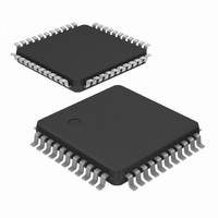
PXAG30KBBD,157 NXP Semiconductors, PXAG30KBBD,157 Datasheet - Page 29

PXAG30KBBD,157
Manufacturer Part Number
PXAG30KBBD,157
Description
IC XA MCU 16BIT ROMLESS 44-LQFP
Manufacturer
NXP Semiconductors
Series
XAr
Datasheet
1.PXAG30KBBD157.pdf
(36 pages)
Specifications of PXAG30KBBD,157
Program Memory Type
ROMless
Package / Case
44-LQFP
Core Processor
XA
Core Size
16-Bit
Speed
30MHz
Connectivity
UART/USART
Peripherals
PWM, WDT
Number Of I /o
32
Ram Size
512 x 8
Voltage - Supply (vcc/vdd)
2.7 V ~ 5.5 V
Oscillator Type
External
Operating Temperature
0°C ~ 70°C
Processor Series
PXAG3x
Core
80C51
Data Bus Width
16 bit
Data Ram Size
512 B
Interface Type
UART
Maximum Clock Frequency
30 MHz
Number Of Programmable I/os
32
Number Of Timers
3
Operating Supply Voltage
2.7 V to 5.5 V
Maximum Operating Temperature
+ 70 C
Mounting Style
SMD/SMT
Minimum Operating Temperature
0 C
Cpu Family
XA
Device Core
80C51
Device Core Size
16b
Frequency (max)
30MHz
Program Memory Size
Not Required
Total Internal Ram Size
512Byte
# I/os (max)
32
Number Of Timers - General Purpose
3
Operating Supply Voltage (typ)
3.3/5V
Operating Supply Voltage (max)
5.5V
Operating Supply Voltage (min)
2.7V
Instruction Set Architecture
CISC
Operating Temp Range
0C to 70C
Operating Temperature Classification
Commercial
Mounting
Surface Mount
Pin Count
44
Package Type
LQFP
Lead Free Status / RoHS Status
Lead free / RoHS Compliant
Eeprom Size
-
Program Memory Size
-
Data Converters
-
Lead Free Status / Rohs Status
Lead free / RoHS Compliant
Other names
568-1300
935270581157
PXAG30KBBD
935270581157
PXAG30KBBD
Available stocks
Company
Part Number
Manufacturer
Quantity
Price
Company:
Part Number:
PXAG30KBBD,157
Manufacturer:
NXP Semiconductors
Quantity:
10 000
Philips Semiconductors
2002 Mar 25
* DATA OUT is either D0–D7 or D0–D15, depending on the bus width (8 or 16 bits).
XA 16-bit microcontroller family
512 B RAM, watchdog, 2 UARTs
ADDRESS BUS
UNMULTIPLEXED
RD, OR PSEN)
BUS STROBE
(WRL, WRH,
MULTIPLEXED
WRL or WRH
ADDRESS
AND DATA
ADDRESS
XTAL1
WAIT
ALE
ALE
t
CRAR
t
AVLL
t
WTH
A4–A11 or A4–A15
t
LLAX
t
AVWL
t
Figure 20. External Data Memory Write Cycle
LLWL
t
QVWX
Figure 21. WAIT Signal Timing
A0 or A1–A3, A12–A19
t
WTL
DATA OUT
t
27
WLWH
*
(The dashed line shows the strobe without WAIT.)
t
UAWH
t
WHQX
XA-G30
SU00709A
Product data
SU00584C


