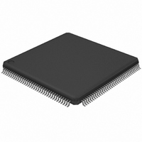
LPC2388FBD144,551 NXP Semiconductors, LPC2388FBD144,551 Datasheet - Page 21

LPC2388FBD144,551
Manufacturer Part Number
LPC2388FBD144,551
Description
IC ARM7 MCU FLASH 512K 144LQFP
Manufacturer
NXP Semiconductors
Series
LPC2300r
Specifications of LPC2388FBD144,551
Program Memory Type
FLASH
Program Memory Size
512KB (512K x 8)
Package / Case
144-LQFP
Core Processor
ARM7
Core Size
16/32-Bit
Speed
72MHz
Connectivity
CAN, EBI/EMI, Ethernet, I²C, Microwire, MMC, SPI, SSI, SSP, UART/USART, USB OTG
Peripherals
Brown-out Detect/Reset, DMA, I²S, POR, PWM, WDT
Number Of I /o
104
Ram Size
98K x 8
Voltage - Supply (vcc/vdd)
3 V ~ 3.6 V
Data Converters
A/D 8x10b; D/A 1x10b
Oscillator Type
Internal
Operating Temperature
-40°C ~ 85°C
Processor Series
LPC23
Core
ARM7TDMI-S
Data Bus Width
16 bit, 32 bit
Data Ram Size
98 KB
Interface Type
CAN/I2C/I2S/SPI/SSP/UART/USB
Maximum Clock Frequency
72 MHz
Number Of Programmable I/os
104
Number Of Timers
4
Operating Supply Voltage
3.3 V
Maximum Operating Temperature
+ 85 C
Mounting Style
SMD/SMT
3rd Party Development Tools
MDK-ARM, RL-ARM, ULINK2, MCB2388, MCB2388U, MCB2388UME
Development Tools By Supplier
OM11012
Minimum Operating Temperature
- 40 C
On-chip Adc
8-ch x 10-bit
On-chip Dac
1-ch x 10-bit
Lead Free Status / RoHS Status
Lead free / RoHS Compliant
For Use With
OM11012 - BOARD EVAL FOR LPC2388568-3999 - BOARD EVAL FOR LPC23 ARM MCU622-1005 - USB IN-CIRCUIT PROG ARM7 LPC2K
Eeprom Size
-
Lead Free Status / Rohs Status
Lead free / RoHS Compliant
Other names
568-4323
935285417551
LPC2388FBD144-S
935285417551
LPC2388FBD144-S
Available stocks
Company
Part Number
Manufacturer
Quantity
Price
Company:
Part Number:
LPC2388FBD144,551
Manufacturer:
NXP Semiconductors
Quantity:
10 000
NXP Semiconductors
LPC2388_0
Preliminary data sheet
7.9.1 Features
7.10 Ethernet
7.9 Fast general purpose parallel I/O
Device pins that are not connected to a specific peripheral function are controlled by the
GPIO registers. Pins may be dynamically configured as inputs or outputs. Separate
registers allow setting or clearing any number of outputs simultaneously. The value of the
output register may be read back as well as the current state of the port pins.
LPC2388 use accelerated GPIO functions:
Additionally, any pin on PORT0 and PORT2 (total of 46 pins) providing a digital function
can be programmed to generate an interrupt on a rising edge, a falling edge, or both. The
edge detection is asynchronous, so it may operate when clocks are not present such as
during Power-down mode. Each enabled interrupt can be used to wake up the chip from
Power-down mode.
The Ethernet block contains a full featured 10 Mbit/s or 100 Mbit/s Ethernet MAC
designed to provide optimized performance through the use of DMA hardware
acceleration. Features include a generous suite of control registers, half or full duplex
operation, flow control, control frames, hardware acceleration for transmit retry, receive
packet filtering and wake-up on LAN activity. Automatic frame transmission and reception
with scatter-gather DMA off-loads many operations from the CPU.
The Ethernet block and the CPU share a dedicated AHB subsystem that is used to access
the Ethernet SRAM for Ethernet data, control, and status information. All other AHB traffic
in the LPC2388 takes place on a different AHB subsystem, effectively separating Ethernet
activity from the rest of the system. The Ethernet DMA can also access off-chip memory
•
•
•
•
•
•
•
•
•
•
•
An interrupt to the processor can be generated on a DMA completion or when a DMA
error has occurred.
Interrupt masking. The DMA error and DMA terminal count interrupt requests can be
masked.
Raw interrupt status. The DMA error and DMA count raw interrupt status can be read
prior to masking.
GPIO registers are relocated to the ARM local bus so that the fastest possible I/O
timing can be achieved.
Mask registers allow treating sets of port bits as a group, leaving other bits
unchanged.
All GPIO registers are byte and half-word addressable.
Entire port value can be written in one instruction.
Bit level set and clear registers allow a single instruction to set or clear any number of
bits in one port.
Direction control of individual bits.
All I/O default to inputs after reset.
Backward compatibility with other earlier devices is maintained with legacy PORT0
and PORT1 registers appearing at the original addresses on the APB bus.
Rev. 00.01 — 23 October 2007
Fast communication chip
LPC2388
© NXP B.V. 2007. All rights reserved.
21 of 57


