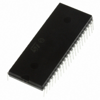
ST72F324BJ6B6 STMicroelectronics, ST72F324BJ6B6 Datasheet - Page 169

ST72F324BJ6B6
Manufacturer Part Number
ST72F324BJ6B6
Description
MCU 8BIT 32KB FLASH/ROM 42-SDIP
Manufacturer
STMicroelectronics
Series
ST7r
Datasheet
1.ST72F324BJ6B6.pdf
(193 pages)
Specifications of ST72F324BJ6B6
Core Processor
ST7
Core Size
8-Bit
Speed
8MHz
Connectivity
SCI, SPI
Peripherals
LVD, POR, PWM, WDT
Number Of I /o
32
Program Memory Size
32KB (32K x 8)
Program Memory Type
FLASH
Ram Size
1K x 8
Voltage - Supply (vcc/vdd)
3.8 V ~ 5.5 V
Data Converters
A/D 12x10b
Oscillator Type
Internal
Operating Temperature
-40°C ~ 85°C
Package / Case
42-SDIP (0.600", 15.24mm)
Controller Family/series
ST7
No. Of I/o's
32
Ram Memory Size
1KB
Cpu Speed
8MHz
No. Of Timers
2
Embedded Interface Type
SCI, SPI
No. Of Pwm Channels
3
Processor Series
ST72F3x
Core
ST7
Data Bus Width
8 bit
Data Ram Size
1 KB
Interface Type
SCI, SPI
Maximum Clock Frequency
8 MHz
Number Of Programmable I/os
32
Number Of Timers
3
Maximum Operating Temperature
+ 85 C
Mounting Style
Through Hole
Development Tools By Supplier
ST7232X-EVAL, ST7MDT20-DVP3, ST7MDT20J-EMU3, STX-RLINK
Minimum Operating Temperature
- 40 C
On-chip Adc
10 bit, 12 Channel
For Use With
497-6421 - BOARD EVAL DGTL BATT CHGR DESIGN497-5046 - KIT TOOL FOR ST7/UPSD/STR7 MCU
Lead Free Status / RoHS Status
Lead free / RoHS Compliant
Eeprom Size
-
Lead Free Status / Rohs Status
Details
Other names
497-5589-5
- Current page: 169 of 193
- Download datasheet (3Mb)
ST72324Bxx
Table 112. 10-bit ADC characteristics (continued)
1. Any added external serial resistor will downgrade the ADC accuracy (especially for resistance greater than 10kΩ). Data
2. Injecting negative current on adjacent pins may result in increased leakage currents. Software filtering of the converted
Symbol
t
ADC
based on characterization results, not tested in production.
analog value is recommended.
Conversion time (Sample + Hold)
f
f
No. of sample capacitor loading cycles
No. of Hold conversion cycles
CPU
ADC
Figure 84. R
1. C
Figure 85. Recommended C
1. This graph shows that, depending on the input signal variation (f
Figure 86. Typical A/D converter application
= 8 MHz, Speed = 0,
= 2 MHz
the pad capacitance (3 pF). A high C
f
stabilization time and decreased to allow the use of a larger serial resistor (R
ADC
PARASITIC
should be reduced.
Parameter
V
AIN
represents the capacitance of the PCB (dependent on soldering and PCB layout quality) plus
AIN
R
max. vs f
AIN
C
AIN
ADC
AINx
AIN
45
40
35
30
25
20
15
10
1000
5
0
100
0.1
with C
PARASITIC
10
1
and R
0
0.01
Conditions
AIN
value will downgrade conversion accuracy. To remedy this,
AIN
V
= 0 pF
DD
10
C
0.1
PARASITIC
values
V
0.6 V
V
0.6 V
f
AIN
T
T
(KHz)
(pF)
(1)
30
1
(1)
2 kΩ (max)
Cain 10 nF
Cain 22 nF
Cain 47 nF
AIN
I
2 MHz
1 MHz
lkg
), C
70
10
Min
AIN
can be increased for
10-bit A/D
conversion
AIN)
Electrical characteristics
Typ
.
7.5
11
4
ST72XXX
Max
C
12 pF
ADC
169/193
1/f
Unit
µs
ADC
Related parts for ST72F324BJ6B6
Image
Part Number
Description
Manufacturer
Datasheet
Request
R

Part Number:
Description:
STMicroelectronics [RIPPLE-CARRY BINARY COUNTER/DIVIDERS]
Manufacturer:
STMicroelectronics
Datasheet:

Part Number:
Description:
STMicroelectronics [LIQUID-CRYSTAL DISPLAY DRIVERS]
Manufacturer:
STMicroelectronics
Datasheet:

Part Number:
Description:
BOARD EVAL FOR MEMS SENSORS
Manufacturer:
STMicroelectronics
Datasheet:

Part Number:
Description:
NPN TRANSISTOR POWER MODULE
Manufacturer:
STMicroelectronics
Datasheet:

Part Number:
Description:
TURBOSWITCH ULTRA-FAST HIGH VOLTAGE DIODE
Manufacturer:
STMicroelectronics
Datasheet:

Part Number:
Description:
Manufacturer:
STMicroelectronics
Datasheet:

Part Number:
Description:
DIODE / SCR MODULE
Manufacturer:
STMicroelectronics
Datasheet:

Part Number:
Description:
DIODE / SCR MODULE
Manufacturer:
STMicroelectronics
Datasheet:

Part Number:
Description:
Search -----> STE16N100
Manufacturer:
STMicroelectronics
Datasheet:

Part Number:
Description:
Search ---> STE53NA50
Manufacturer:
STMicroelectronics
Datasheet:

Part Number:
Description:
NPN Transistor Power Module
Manufacturer:
STMicroelectronics
Datasheet:


