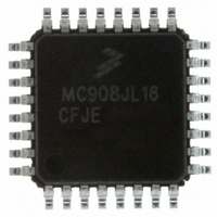
MC908JL16CFJER Freescale Semiconductor, MC908JL16CFJER Datasheet - Page 124

MC908JL16CFJER
Manufacturer Part Number
MC908JL16CFJER
Description
IC MCU 8BIT 16K FLASH 32-LQFP
Manufacturer
Freescale Semiconductor
Series
HC08r
Datasheet
1.MC908JL16CFJER.pdf
(230 pages)
Specifications of MC908JL16CFJER
Core Processor
HC08
Core Size
8-Bit
Speed
8MHz
Connectivity
I²C, SCI
Peripherals
LED, LVD, POR, PWM
Number Of I /o
26
Program Memory Size
16KB (16K x 8)
Program Memory Type
FLASH
Ram Size
512 x 8
Voltage - Supply (vcc/vdd)
2.7 V ~ 5.5 V
Data Converters
A/D 13x10b
Oscillator Type
Internal
Operating Temperature
-40°C ~ 85°C
Package / Case
32-LQFP
Controller Family/series
HC08
No. Of I/o's
26
Ram Memory Size
512Byte
Cpu Speed
8MHz
No. Of Timers
2
Digital Ic Case Style
LQFP
Rohs Compliant
Yes
Processor Series
HC08JL
Core
HC08
Data Bus Width
8 bit
Data Ram Size
512 B
Interface Type
SCI
Maximum Clock Frequency
8 MHz
Number Of Programmable I/os
26
Number Of Timers
4
Maximum Operating Temperature
+ 85 C
Mounting Style
SMD/SMT
Development Tools By Supplier
FSICEBASE, DEMO908JL16E, M68CBL05CE
Minimum Operating Temperature
- 40 C
On-chip Adc
10 bit, 13 Channel
For Use With
DEMO908JL16E - BOARD DEMO FOR MC908JL16
Lead Free Status / RoHS Status
Lead free / RoHS Compliant
Eeprom Size
-
Lead Free Status / Rohs Status
Details
Other names
MC908JL16CFJERTR
Available stocks
Company
Part Number
Manufacturer
Quantity
Price
Company:
Part Number:
MC908JL16CFJER
Manufacturer:
Freescale Semiconductor
Quantity:
29 890
Company:
Part Number:
MC908JL16CFJER
Manufacturer:
Freescale
Quantity:
198
Company:
Part Number:
MC908JL16CFJER
Manufacturer:
Freescale Semiconductor
Quantity:
10 000
Analog-to-Digital Converter (ADC)
9.3 Functional Description
The ADC10 uses successive approximation to convert the input sample taken from ADVIN to a digital
representation. The approximation is taken and then rounded to the nearest 10- or 8-bit value to provide
greater accuracy and to provide a more robust mechanism for achieving the ideal code-transition voltage.
Figure 9-2
For proper conversion, the voltage on ADVIN must fall between V
or exceeds V
a 8-bit representation. If ADVIN is equal to or less than V
Input voltages between V
The ADC10 can perform an analog-to-digital conversion on one of the software selectable channels. The
output of the input multiplexer (ADVIN) is converted by a successive approximation algorithm into a 10-bit
digital result. When the conversion is completed, the result is placed in the data registers (ADRH and
ADRL). In 8-bit mode, the result is rounded to 8 bits and placed in ADRL. The conversion complete flag
is then set and an interrupt is generated if the interrupt has been enabled.
124
MCU STOP
ADHWT
V
V
REFH
REFL
AD0
ADn
shows a block diagram of the ADC10.
REFH
, the converter circuit converts the signal to $3FF for a 10-bit representation or $FF for
Input voltage must not exceed the analog supply voltages.
1
ADVIN
REFH
ADCSC
2
and V
CONTROL SEQUENCER
Figure 9-2. ADC10 Block Diagram
MC68HC908JL16 Data Sheet, Rev. 1.1
DATA REGISTERS ADRH:ADRL
REFL
SAR CONVERTER
are straight-line linear conversions.
NOTE
ADCK
ADCLK
CLOCK
DIVIDE
REFL
, the converter circuit converts it to $000.
COCO
AIEN
REFH
1
2
ACLK
ACLKEN
and V
REFL
BUS CLOCK
ALTERNATE CLOCK SOURCE
GENERATOR
ASYNC
CLOCK
. If ADVIN is equal to
Freescale Semiconductor
INTERRUPT


