C8051F819-GM Silicon Laboratories Inc, C8051F819-GM Datasheet - Page 10
C8051F819-GM
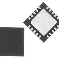
Manufacturer Part Number
C8051F819-GM
Description
IC MCU 8BIT 8KB FLASH 20QFN
Manufacturer
Silicon Laboratories Inc
Series
C8051F81xr
Datasheet
1.C8051F800DK.pdf
(250 pages)
Specifications of C8051F819-GM
Core Processor
8051
Core Size
8-Bit
Speed
25MHz
Connectivity
SMBus (2-Wire/I²C), SPI, UART/USART
Peripherals
Cap Sense, POR, PWM, WDT
Number Of I /o
17
Program Memory Size
8KB (8K x 8)
Program Memory Type
FLASH
Ram Size
512 x 8
Voltage - Supply (vcc/vdd)
1.8 V ~ 3.6 V
Oscillator Type
Internal
Operating Temperature
-40°C ~ 85°C
Package / Case
20-QFN
Processor Series
C8051F8x
Core
8051
Data Bus Width
16 bit
Data Ram Size
512 B
Interface Type
I2C, SPI, UART
Maximum Clock Frequency
25 MHz
Number Of Programmable I/os
17
Number Of Timers
3
Operating Supply Voltage
1.8 V to 3.6 V
Maximum Operating Temperature
+ 125 C
Mounting Style
SMD/SMT
3rd Party Development Tools
PK51, CA51, A51, ULINK2
Development Tools By Supplier
C8051F800DK
Minimum Operating Temperature
- 55 C
Package
20QFN EP
Device Core
8051
Family Name
C8051F8xx
Maximum Speed
25 MHz
Lead Free Status / RoHS Status
Lead free / RoHS Compliant
Eeprom Size
-
Data Converters
-
Lead Free Status / Rohs Status
Details
Other names
336-1799-5


C8051F80x-83x
14. CIP-51 Microcontroller
15. Memory Organization
16. In-System Device Identification
17. Special Function Registers
18. Interrupts
19. Flash Memory
20. Power Management Modes
21. Reset Sources
22. Oscillators and Clock Selection
23. Port Input/Output
24. Cyclic Redundancy Check Unit (CRC0)
25. Enhanced Serial Peripheral Interface (SPI0)
26. SMBus
10
Figure 13.1. CS0 Block Diagram ............................................................................. 71
Figure 13.2. Auto-Scan Example ............................................................................. 73
Figure 13.3. CS0 Multiplexer Block Diagram ........................................................... 80
Figure 14.1. CIP-51 Block Diagram ......................................................................... 82
Figure 15.1. C8051F80x-83x Memory Map ............................................................. 92
Figure 15.2. Flash Program Memory Map ............................................................... 93
Figure 21.1. Reset Sources ................................................................................... 123
Figure 21.2. Power-On and VDD Monitor Reset Timing ....................................... 124
Figure 22.1. Oscillator Options .............................................................................. 129
Figure 22.2. External 32.768 kHz Quartz Crystal Oscillator Connection Diagram 136
Figure 23.1. Port I/O Functional Block Diagram .................................................... 138
Figure 23.2. Port I/O Cell Block Diagram .............................................................. 139
Figure 23.3. Port I/O Overdrive Current ................................................................ 140
Figure 23.4. Priority Crossbar Decoder Potential Pin Assignments ...................... 144
Figure 23.5. Priority Crossbar Decoder Example 1—No Skipped Pins ................. 145
Figure 23.6. Priority Crossbar Decoder Example 2—Skipping Pins ...................... 146
Figure 24.1. CRC0 Block Diagram ........................................................................ 159
Figure 25.1. SPI Block Diagram ............................................................................ 167
Figure 25.2. Multiple-Master Mode Connection Diagram ...................................... 169
Figure 25.3. 3-Wire Single Master and 3-Wire Single Slave Mode Connection Diagram
Figure 25.4. 4-Wire Single Master Mode and 4-Wire Slave Mode Connection Diagram
Figure 25.5. Master Mode Data/Clock Timing ....................................................... 172
Figure 25.6. Slave Mode Data/Clock Timing (CKPHA = 0) ................................... 172
Figure 25.7. Slave Mode Data/Clock Timing (CKPHA = 1) ................................... 173
Figure 25.8. SPI Master Timing (CKPHA = 0) ....................................................... 177
Figure 25.9. SPI Master Timing (CKPHA = 1) ....................................................... 177
Figure 25.10. SPI Slave Timing (CKPHA = 0) ....................................................... 178
Figure 25.11. SPI Slave Timing (CKPHA = 1) ....................................................... 178
Figure 26.1. SMBus Block Diagram ...................................................................... 180
Figure 26.2. Typical SMBus Configuration ............................................................ 181
170
169
Rev. 1.0
Related parts for C8051F819-GM
Image
Part Number
Description
Manufacturer
Datasheet
Request
R

Part Number:
Description:
SMD/C°/SINGLE-ENDED OUTPUT SILICON OSCILLATOR
Manufacturer:
Silicon Laboratories Inc
Part Number:
Description:
Manufacturer:
Silicon Laboratories Inc
Datasheet:
Part Number:
Description:
N/A N/A/SI4010 AES KEYFOB DEMO WITH LCD RX
Manufacturer:
Silicon Laboratories Inc
Datasheet:
Part Number:
Description:
N/A N/A/SI4010 SIMPLIFIED KEY FOB DEMO WITH LED RX
Manufacturer:
Silicon Laboratories Inc
Datasheet:
Part Number:
Description:
N/A/-40 TO 85 OC/EZLINK MODULE; F930/4432 HIGH BAND (REV E/B1)
Manufacturer:
Silicon Laboratories Inc
Part Number:
Description:
EZLink Module; F930/4432 Low Band (rev e/B1)
Manufacturer:
Silicon Laboratories Inc
Part Number:
Description:
I°/4460 10 DBM RADIO TEST CARD 434 MHZ
Manufacturer:
Silicon Laboratories Inc
Part Number:
Description:
I°/4461 14 DBM RADIO TEST CARD 868 MHZ
Manufacturer:
Silicon Laboratories Inc
Part Number:
Description:
I°/4463 20 DBM RFSWITCH RADIO TEST CARD 460 MHZ
Manufacturer:
Silicon Laboratories Inc
Part Number:
Description:
I°/4463 20 DBM RADIO TEST CARD 868 MHZ
Manufacturer:
Silicon Laboratories Inc
Part Number:
Description:
I°/4463 27 DBM RADIO TEST CARD 868 MHZ
Manufacturer:
Silicon Laboratories Inc
Part Number:
Description:
I°/4463 SKYWORKS 30 DBM RADIO TEST CARD 915 MHZ
Manufacturer:
Silicon Laboratories Inc
Part Number:
Description:
N/A N/A/-40 TO 85 OC/4463 RFMD 30 DBM RADIO TEST CARD 915 MHZ
Manufacturer:
Silicon Laboratories Inc
Part Number:
Description:
I°/4463 20 DBM RADIO TEST CARD 169 MHZ
Manufacturer:
Silicon Laboratories Inc