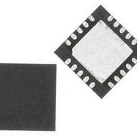
C8051F819-GM Silicon Laboratories Inc, C8051F819-GM Datasheet - Page 115

C8051F819-GM
Manufacturer Part Number
C8051F819-GM
Description
IC MCU 8BIT 8KB FLASH 20QFN
Manufacturer
Silicon Laboratories Inc
Series
C8051F81xr
Datasheet
1.C8051F800DK.pdf
(250 pages)
Specifications of C8051F819-GM
Core Processor
8051
Core Size
8-Bit
Speed
25MHz
Connectivity
SMBus (2-Wire/I²C), SPI, UART/USART
Peripherals
Cap Sense, POR, PWM, WDT
Number Of I /o
17
Program Memory Size
8KB (8K x 8)
Program Memory Type
FLASH
Ram Size
512 x 8
Voltage - Supply (vcc/vdd)
1.8 V ~ 3.6 V
Oscillator Type
Internal
Operating Temperature
-40°C ~ 85°C
Package / Case
20-QFN
Processor Series
C8051F8x
Core
8051
Data Bus Width
16 bit
Data Ram Size
512 B
Interface Type
I2C, SPI, UART
Maximum Clock Frequency
25 MHz
Number Of Programmable I/os
17
Number Of Timers
3
Operating Supply Voltage
1.8 V to 3.6 V
Maximum Operating Temperature
+ 125 C
Mounting Style
SMD/SMT
3rd Party Development Tools
PK51, CA51, A51, ULINK2
Development Tools By Supplier
C8051F800DK
Minimum Operating Temperature
- 55 C
Package
20QFN EP
Device Core
8051
Family Name
C8051F8xx
Maximum Speed
25 MHz
Lead Free Status / RoHS Status
Lead free / RoHS Compliant
Eeprom Size
-
Data Converters
-
Lead Free Status / Rohs Status
Details
Other names
336-1799-5
- Current page: 115 of 250
- Download datasheet (2Mb)
unlocked pages, and user firmware executing on locked pages. Table 19.1 summarizes the Flash security
features of the C8051F80x-83x devices.
19.4. Flash Write and Erase Guidelines
Any system which contains routines which write or erase Flash memory from software involves some risk
that the write or erase routines will execute unintentionally if the CPU is operating outside its specified
operating range of VDD, system clock frequency, or temperature. This accidental execution of Flash modi-
fying code can result in alteration of Flash memory contents causing a system failure that is only recover-
able by re-Flashing the code in the device.
To help prevent the accidental modification of Flash by firmware, the VDD Monitor must be enabled and
enabled as a reset source on C8051F80x-83x devices for the Flash to be successfully modified. If either
Read, Write or Erase unlocked pages
(except page with Lock Byte)
Read, Write or Erase locked pages
(except page with Lock Byte)
Read or Write page containing Lock Byte
(if no pages are locked)
Read or Write page containing Lock Byte
(if any page is locked)
Read contents of Lock Byte
(if no pages are locked)
Read contents of Lock Byte
(if any page is locked)
Erase page containing Lock Byte
(if no pages are locked)
Erase page containing Lock Byte—Unlock all
pages (if any page is locked)
Lock additional pages
(change 1s to 0s in the Lock Byte)
Unlock individual pages
(change 0s to 1s in the Lock Byte)
Read, Write or Erase Reserved Area
C2DE—C2 Device Erase (Erases all Flash pages including the page containing the Lock Byte)
FEDR—Not permitted; Causes Flash Error Device Reset (FERROR bit in RSTSRC is 1 after reset)
All prohibited operations that are performed via the C2 interface are ignored (do not cause device
reset).
Locking any Flash page also locks the page containing the Lock Byte.
Once written to, the Lock Byte cannot be modified except by performing a C2 Device Erase.
If user code writes to the Lock Byte, the Lock does not take effect until the next device reset.
Action
Table 19.1. Flash Security Summary
Rev. 1.0
Permitted
Not Permitted FEDR
Permitted
Not Permitted FEDR
Permitted
Not Permitted FEDR
Permitted
Only by C2DE FEDR
Not Permitted FEDR
Not Permitted FEDR
Not Permitted FEDR
C2 Debug
Interface
Permitted
Permitted
Permitted
FEDR
an unlocked page a locked page
User Firmware executing from:
C8051F80x-83x
Permitted
Permitted
Permitted
Permitted
Permitted
Permitted
FEDR
FEDR
FEDR
FEDR
FEDR
115
Related parts for C8051F819-GM
Image
Part Number
Description
Manufacturer
Datasheet
Request
R
Part Number:
Description:
SMD/C°/SINGLE-ENDED OUTPUT SILICON OSCILLATOR
Manufacturer:
Silicon Laboratories Inc
Part Number:
Description:
Manufacturer:
Silicon Laboratories Inc
Datasheet:
Part Number:
Description:
N/A N/A/SI4010 AES KEYFOB DEMO WITH LCD RX
Manufacturer:
Silicon Laboratories Inc
Datasheet:
Part Number:
Description:
N/A N/A/SI4010 SIMPLIFIED KEY FOB DEMO WITH LED RX
Manufacturer:
Silicon Laboratories Inc
Datasheet:
Part Number:
Description:
N/A/-40 TO 85 OC/EZLINK MODULE; F930/4432 HIGH BAND (REV E/B1)
Manufacturer:
Silicon Laboratories Inc
Part Number:
Description:
EZLink Module; F930/4432 Low Band (rev e/B1)
Manufacturer:
Silicon Laboratories Inc
Part Number:
Description:
I°/4460 10 DBM RADIO TEST CARD 434 MHZ
Manufacturer:
Silicon Laboratories Inc
Part Number:
Description:
I°/4461 14 DBM RADIO TEST CARD 868 MHZ
Manufacturer:
Silicon Laboratories Inc
Part Number:
Description:
I°/4463 20 DBM RFSWITCH RADIO TEST CARD 460 MHZ
Manufacturer:
Silicon Laboratories Inc
Part Number:
Description:
I°/4463 20 DBM RADIO TEST CARD 868 MHZ
Manufacturer:
Silicon Laboratories Inc
Part Number:
Description:
I°/4463 27 DBM RADIO TEST CARD 868 MHZ
Manufacturer:
Silicon Laboratories Inc
Part Number:
Description:
I°/4463 SKYWORKS 30 DBM RADIO TEST CARD 915 MHZ
Manufacturer:
Silicon Laboratories Inc
Part Number:
Description:
N/A N/A/-40 TO 85 OC/4463 RFMD 30 DBM RADIO TEST CARD 915 MHZ
Manufacturer:
Silicon Laboratories Inc
Part Number:
Description:
I°/4463 20 DBM RADIO TEST CARD 169 MHZ
Manufacturer:
Silicon Laboratories Inc


