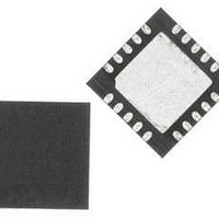
C8051F819-GM Silicon Laboratories Inc, C8051F819-GM Datasheet - Page 60

C8051F819-GM
Manufacturer Part Number
C8051F819-GM
Description
IC MCU 8BIT 8KB FLASH 20QFN
Manufacturer
Silicon Laboratories Inc
Series
C8051F81xr
Datasheet
1.C8051F800DK.pdf
(250 pages)
Specifications of C8051F819-GM
Core Processor
8051
Core Size
8-Bit
Speed
25MHz
Connectivity
SMBus (2-Wire/I²C), SPI, UART/USART
Peripherals
Cap Sense, POR, PWM, WDT
Number Of I /o
17
Program Memory Size
8KB (8K x 8)
Program Memory Type
FLASH
Ram Size
512 x 8
Voltage - Supply (vcc/vdd)
1.8 V ~ 3.6 V
Oscillator Type
Internal
Operating Temperature
-40°C ~ 85°C
Package / Case
20-QFN
Processor Series
C8051F8x
Core
8051
Data Bus Width
16 bit
Data Ram Size
512 B
Interface Type
I2C, SPI, UART
Maximum Clock Frequency
25 MHz
Number Of Programmable I/os
17
Number Of Timers
3
Operating Supply Voltage
1.8 V to 3.6 V
Maximum Operating Temperature
+ 125 C
Mounting Style
SMD/SMT
3rd Party Development Tools
PK51, CA51, A51, ULINK2
Development Tools By Supplier
C8051F800DK
Minimum Operating Temperature
- 55 C
Package
20QFN EP
Device Core
8051
Family Name
C8051F8xx
Maximum Speed
25 MHz
Lead Free Status / RoHS Status
Lead free / RoHS Compliant
Eeprom Size
-
Data Converters
-
Lead Free Status / Rohs Status
Details
Other names
336-1799-5
- Current page: 60 of 250
- Download datasheet (2Mb)
C8051F80x-83x
10. Voltage and Ground Reference Options
The voltage reference MUX is configurable to use an externally connected voltage reference, the on-chip
voltage reference, or one of two power supply voltages (see Figure 10.1). The ground reference MUX
allows the ground reference for ADC0 to be selected between the ground pin (GND) or a port pin dedi-
cated to analog ground (P0.1/AGND).
The voltage and ground reference options are configured using the REF0CN SFR described on page 62.
Electrical specifications are can be found in the Electrical Specifications Chapter.
Important Note About the V
inputs. When using an external voltage reference, P0.0/VREF should be configured as an analog input and
skipped by the Digital Crossbar. When using AGND as the ground reference to ADC0, P0.1/AGND should
be configured as an analog input and skipped by the Digital Crossbar. Refer to Section “23. Port Input/Out-
put” on page 138 for complete Port I/O configuration details. The external reference voltage must be within
the range 0 V
GND.
60
4.7F
Bypass Capacitors
Recommended
GND
VDD
+
R1
Reference
External
Voltage
Circuit
0.1F
REF
Figure 10.1. Voltage Reference Functional Block Diagram
V
P0.1/AGND
P0.0/VREF
DD
and the external ground reference must be at the same DC voltage potential as
GND
V
DD
REF
and AGND Inputs: Port pins are used as the external V
Regulated Digital Supply
High Speed Reference
REF0CN
Rev. 1.0
Internal 1.65V
Internal 1.8V
IOSCEN
EN
EN
REFGND
Bias Generator
Temp Sensor
00
01
10
11
0
1
To Analog Mux
REF
To ADC, Internal
Oscillator,
Reference,
TempSensor
and AGND
Related parts for C8051F819-GM
Image
Part Number
Description
Manufacturer
Datasheet
Request
R
Part Number:
Description:
SMD/C°/SINGLE-ENDED OUTPUT SILICON OSCILLATOR
Manufacturer:
Silicon Laboratories Inc
Part Number:
Description:
Manufacturer:
Silicon Laboratories Inc
Datasheet:
Part Number:
Description:
N/A N/A/SI4010 AES KEYFOB DEMO WITH LCD RX
Manufacturer:
Silicon Laboratories Inc
Datasheet:
Part Number:
Description:
N/A N/A/SI4010 SIMPLIFIED KEY FOB DEMO WITH LED RX
Manufacturer:
Silicon Laboratories Inc
Datasheet:
Part Number:
Description:
N/A/-40 TO 85 OC/EZLINK MODULE; F930/4432 HIGH BAND (REV E/B1)
Manufacturer:
Silicon Laboratories Inc
Part Number:
Description:
EZLink Module; F930/4432 Low Band (rev e/B1)
Manufacturer:
Silicon Laboratories Inc
Part Number:
Description:
I°/4460 10 DBM RADIO TEST CARD 434 MHZ
Manufacturer:
Silicon Laboratories Inc
Part Number:
Description:
I°/4461 14 DBM RADIO TEST CARD 868 MHZ
Manufacturer:
Silicon Laboratories Inc
Part Number:
Description:
I°/4463 20 DBM RFSWITCH RADIO TEST CARD 460 MHZ
Manufacturer:
Silicon Laboratories Inc
Part Number:
Description:
I°/4463 20 DBM RADIO TEST CARD 868 MHZ
Manufacturer:
Silicon Laboratories Inc
Part Number:
Description:
I°/4463 27 DBM RADIO TEST CARD 868 MHZ
Manufacturer:
Silicon Laboratories Inc
Part Number:
Description:
I°/4463 SKYWORKS 30 DBM RADIO TEST CARD 915 MHZ
Manufacturer:
Silicon Laboratories Inc
Part Number:
Description:
N/A N/A/-40 TO 85 OC/4463 RFMD 30 DBM RADIO TEST CARD 915 MHZ
Manufacturer:
Silicon Laboratories Inc
Part Number:
Description:
I°/4463 20 DBM RADIO TEST CARD 169 MHZ
Manufacturer:
Silicon Laboratories Inc


