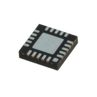
C8051F813-GM Silicon Laboratories Inc, C8051F813-GM Datasheet - Page 28

C8051F813-GM
Manufacturer Part Number
C8051F813-GM
Description
IC MCU 8BIT 8KB FLASH 20QFN
Manufacturer
Silicon Laboratories Inc
Series
C8051F81xr
Datasheet
1.C8051F800DK.pdf
(250 pages)
Specifications of C8051F813-GM
Core Processor
8051
Core Size
8-Bit
Speed
25MHz
Connectivity
SMBus (2-Wire/I²C), SPI, UART/USART
Peripherals
Cap Sense, POR, PWM, Temp Sensor, WDT
Number Of I /o
17
Program Memory Size
8KB (8K x 8)
Program Memory Type
FLASH
Ram Size
512 x 8
Voltage - Supply (vcc/vdd)
1.8 V ~ 3.6 V
Data Converters
A/D 16x10b
Oscillator Type
Internal
Operating Temperature
-40°C ~ 85°C
Package / Case
20-QFN
Processor Series
C8051F8x
Core
8051
Data Bus Width
16 bit
Data Ram Size
512 B
Interface Type
I2C, SPI, UART
Maximum Clock Frequency
25 MHz
Number Of Programmable I/os
17
Number Of Timers
3
Operating Supply Voltage
1.8 V to 3.6 V
Maximum Operating Temperature
+ 125 C
Mounting Style
SMD/SMT
3rd Party Development Tools
PK51, CA51, A51, ULINK2
Development Tools By Supplier
C8051F800DK
Minimum Operating Temperature
- 55 C
On-chip Adc
10 bit, 16 Channel
Lead Free Status / RoHS Status
Lead free / RoHS Compliant
Eeprom Size
-
Lead Free Status / Rohs Status
Details
Other names
336-1786-5
- Current page: 28 of 250
- Download datasheet (2Mb)
C8051F80x-83x
3. Pin Definitions
28
XTAL1
XTAL2
Name
C2CK
VREF
P2.0/
P0.0/
P0.2/
P0.3/
GND
RST/
P0.1
P0.4
C2D
V
DD
QSOP-24
Pin
23
22
5
6
7
8
4
3
2
Table 3.1. Pin Definitions for the C8051F80x-83x
QFN-20
Pin
20
19
18
17
2
3
4
5
1
SOIC-16
Pin
16
15
4
5
6
7
3
2
1
D I/O or
D I/O or
D I/O or
D I/O or
D I/O or
A I/O or
Type
D I/O
D I/O
D I/O
D I/O
A In
A In
A In
A In
A In
A In
D In
A In
Rev. 1.0
Description
Ground.
This ground connection is required. The center
pad may optionally be connected to ground as
well on the QFN-20 packages.
Power Supply Voltage.
Device Reset. Open-drain output of internal
POR or V
tiate a system reset by driving this pin low for at
least 10 µs.
Clock signal for the C2 Debug Interface.
Bi-directional data signal for the C2 Debug Inter-
face. Shared with P2.0 on 20-pin packaging and
P2.4 on 24-pin packaging.
Bi-directional data signal for the C2 Debug Inter-
face. Shared with P2.0 on 20-pin packaging and
P2.4 on 24-pin packaging.
Port 0.0.
External VREF input.
Port 0.1.
Port 0.2.
External Clock Input. This pin is the external
oscillator return for a crystal or resonator.
Port 0.3.
External Clock Output. For an external crystal or
resonator, this pin is the excitation driver. This
pin is the external clock input for CMOS, capaci-
tor, or RC oscillator configurations.
Port 0.4.
DD
monitor. An external source can ini-
Related parts for C8051F813-GM
Image
Part Number
Description
Manufacturer
Datasheet
Request
R
Part Number:
Description:
SMD/C°/SINGLE-ENDED OUTPUT SILICON OSCILLATOR
Manufacturer:
Silicon Laboratories Inc
Part Number:
Description:
Manufacturer:
Silicon Laboratories Inc
Datasheet:
Part Number:
Description:
N/A N/A/SI4010 AES KEYFOB DEMO WITH LCD RX
Manufacturer:
Silicon Laboratories Inc
Datasheet:
Part Number:
Description:
N/A N/A/SI4010 SIMPLIFIED KEY FOB DEMO WITH LED RX
Manufacturer:
Silicon Laboratories Inc
Datasheet:
Part Number:
Description:
N/A/-40 TO 85 OC/EZLINK MODULE; F930/4432 HIGH BAND (REV E/B1)
Manufacturer:
Silicon Laboratories Inc
Part Number:
Description:
EZLink Module; F930/4432 Low Band (rev e/B1)
Manufacturer:
Silicon Laboratories Inc
Part Number:
Description:
I°/4460 10 DBM RADIO TEST CARD 434 MHZ
Manufacturer:
Silicon Laboratories Inc
Part Number:
Description:
I°/4461 14 DBM RADIO TEST CARD 868 MHZ
Manufacturer:
Silicon Laboratories Inc
Part Number:
Description:
I°/4463 20 DBM RFSWITCH RADIO TEST CARD 460 MHZ
Manufacturer:
Silicon Laboratories Inc
Part Number:
Description:
I°/4463 20 DBM RADIO TEST CARD 868 MHZ
Manufacturer:
Silicon Laboratories Inc
Part Number:
Description:
I°/4463 27 DBM RADIO TEST CARD 868 MHZ
Manufacturer:
Silicon Laboratories Inc
Part Number:
Description:
I°/4463 SKYWORKS 30 DBM RADIO TEST CARD 915 MHZ
Manufacturer:
Silicon Laboratories Inc
Part Number:
Description:
N/A N/A/-40 TO 85 OC/4463 RFMD 30 DBM RADIO TEST CARD 915 MHZ
Manufacturer:
Silicon Laboratories Inc
Part Number:
Description:
I°/4463 20 DBM RADIO TEST CARD 169 MHZ
Manufacturer:
Silicon Laboratories Inc


