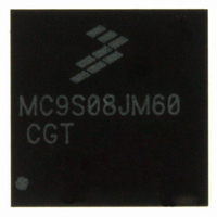
MC9S08JM60CGT Freescale Semiconductor, MC9S08JM60CGT Datasheet - Page 146

MC9S08JM60CGT
Manufacturer Part Number
MC9S08JM60CGT
Description
IC MCU 8BIT 60K FLASH 48-QFN
Manufacturer
Freescale Semiconductor
Series
HCS08r
Datasheet
1.MC9S08JM32CLD.pdf
(388 pages)
Specifications of MC9S08JM60CGT
Core Processor
HCS08
Core Size
8-Bit
Speed
48MHz
Connectivity
I²C, LIN, SCI, SPI, USB
Peripherals
LVD, POR, PWM, WDT
Number Of I /o
37
Program Memory Size
60KB (60K x 8)
Program Memory Type
FLASH
Ram Size
4K x 8
Voltage - Supply (vcc/vdd)
2.7 V ~ 5.5 V
Data Converters
A/D 8x12b
Oscillator Type
External
Operating Temperature
-40°C ~ 85°C
Package / Case
48-QFN
Processor Series
S08JM
Core
HCS08
Data Bus Width
8 bit
Data Ram Size
4 KB
Interface Type
SCI/SPI
Maximum Clock Frequency
24 MHz
Number Of Programmable I/os
37
Number Of Timers
8
Maximum Operating Temperature
+ 85 C
Mounting Style
SMD/SMT
3rd Party Development Tools
EWS08
Development Tools By Supplier
DEMOJM, DEMOJMSKT, DEMOFLEXISJMSD, DEMO9S08JM16
Minimum Operating Temperature
- 40 C
On-chip Adc
8-ch x 12-bit
Cpu Family
HCS08
Device Core Size
8b
Frequency (max)
24MHz
Total Internal Ram Size
4KB
# I/os (max)
37
Number Of Timers - General Purpose
8
Operating Supply Voltage (typ)
3.3/5V
Operating Supply Voltage (max)
5.5V
Operating Supply Voltage (min)
2.7V
Instruction Set Architecture
CISC
Operating Temp Range
-40C to 85C
Operating Temperature Classification
Industrial
Mounting
Surface Mount
Pin Count
48
Package Type
QFN EP
Package
48QFN EP
Family Name
HCS08
Maximum Speed
24 MHz
Operating Supply Voltage
3.3|5 V
For Use With
DEMOJM - KIT DEMO FOR JM MCU FAMILYDEMOJMSKT - BOARD DEMO S08JM CARD W/SOCKET
Lead Free Status / RoHS Status
Lead free / RoHS Compliant
Eeprom Size
-
Lead Free Status / Rohs Status
Lead free / RoHS Compliant
Available stocks
Company
Part Number
Manufacturer
Quantity
Price
- Current page: 146 of 388
- Download datasheet (5Mb)
Analog-to-Digital Converter (S08ADC12V1)
10.3.8
The pin control registers disable the I/O port control of MCU pins used as analog inputs. APCTL1 is used
to control the pins associated with channels 0–7 of the ADC module.
146
ADICLK
MODE
Field
3:2
1:0
Reset:
W
R
Pin Control 1 Register (APCTL1)
Conversion Mode Selection. MODE bits are used to select between 12-, 10-, or 8-bit operation. See
Input Clock Select. ADICLK bits select the input clock source to generate the internal clock ADCK. See
Table
ADPC7
10-9.
7
0
Table 10-6. ADCCFG Register Field Descriptions (continued)
ADICLK
MODE
ADIV
00
01
10
11
00
01
10
11
00
01
10
11
ADPC6
0
6
Figure 10-10. Pin Control 1 Register (APCTL1)
8-bit conversion (N=8)
12-bit conversion (N=12)
10-bit conversion (N=10)
Reserved
Bus clock
Bus clock divided by 2
Alternate clock (ALTCLK)
Asynchronous clock (ADACK)
MC9S08JM60 Series Data Sheet, Rev. 3
ADPC5
Table 10-7. Clock Divide Select
Table 10-8. Conversion Modes
Table 10-9. Input Clock Select
0
5
Divide Ratio
1
2
4
8
ADPC4
Selected Clock Source
0
4
Mode Description
Description
ADPC3
0
3
Input clock ÷ 2
Input clock ÷ 4
Input clock ÷ 8
Clock Rate
Input clock
ADPC2
0
2
ADPC1
Freescale Semiconductor
0
1
ADPC0
Table
0
0
10-8.
Related parts for MC9S08JM60CGT
Image
Part Number
Description
Manufacturer
Datasheet
Request
R
Part Number:
Description:
Manufacturer:
Freescale Semiconductor, Inc
Datasheet:
Part Number:
Description:
Manufacturer:
Freescale Semiconductor, Inc
Datasheet:
Part Number:
Description:
Manufacturer:
Freescale Semiconductor, Inc
Datasheet:
Part Number:
Description:
Manufacturer:
Freescale Semiconductor, Inc
Datasheet:
Part Number:
Description:
Manufacturer:
Freescale Semiconductor, Inc
Datasheet:
Part Number:
Description:
Manufacturer:
Freescale Semiconductor, Inc
Datasheet:
Part Number:
Description:
Manufacturer:
Freescale Semiconductor, Inc
Datasheet:
Part Number:
Description:
Manufacturer:
Freescale Semiconductor, Inc
Datasheet:
Part Number:
Description:
Manufacturer:
Freescale Semiconductor, Inc
Datasheet:
Part Number:
Description:
Manufacturer:
Freescale Semiconductor, Inc
Datasheet:
Part Number:
Description:
Manufacturer:
Freescale Semiconductor, Inc
Datasheet:
Part Number:
Description:
Manufacturer:
Freescale Semiconductor, Inc
Datasheet:
Part Number:
Description:
Manufacturer:
Freescale Semiconductor, Inc
Datasheet:
Part Number:
Description:
Manufacturer:
Freescale Semiconductor, Inc
Datasheet:
Part Number:
Description:
Manufacturer:
Freescale Semiconductor, Inc
Datasheet:


