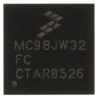
MCHC908JW32FC Freescale Semiconductor, MCHC908JW32FC Datasheet - Page 91

MCHC908JW32FC
Manufacturer Part Number
MCHC908JW32FC
Description
IC MCU 32K FLASH 8MHZ 48-QFN
Manufacturer
Freescale Semiconductor
Series
HC08r
Datasheet
1.RD3152MMA7260Q.pdf
(232 pages)
Specifications of MCHC908JW32FC
Core Processor
HC08
Core Size
8-Bit
Speed
8MHz
Connectivity
SPI, USB
Peripherals
LED, LVD, POR, PWM
Number Of I /o
29
Program Memory Size
32KB (32K x 8)
Program Memory Type
FLASH
Ram Size
1K x 8
Voltage - Supply (vcc/vdd)
3.5 V ~ 5.5 V
Oscillator Type
Internal
Operating Temperature
0°C ~ 70°C
Package / Case
48-QFN
Controller Family/series
HC08
No. Of I/o's
29
Ram Memory Size
1KB
Cpu Speed
8MHz
No. Of Timers
1
Embedded Interface Type
SPI, USB
Rohs Compliant
Yes
Processor Series
HC08JW
Core
HC08
Data Bus Width
8 bit
Data Ram Size
1 KB
Interface Type
SPI, USB
Number Of Programmable I/os
29
Number Of Timers
2
Maximum Operating Temperature
+ 70 C
Mounting Style
SMD/SMT
Development Tools By Supplier
FSICEBASE, DEMO908GZ60E, M68EML08GZE, KITUSBSPIDGLEVME, KITUSBSPIEVME, KIT33810EKEVME
Minimum Operating Temperature
0 C
Lead Free Status / RoHS Status
Lead free / RoHS Compliant
Eeprom Size
-
Data Converters
-
Lead Free Status / Rohs Status
Details
- Current page: 91 of 232
- Download datasheet (3Mb)
PIN — External Reset Bit
COP — Computer Operating Properly Reset Bit
ILOP — Illegal Opcode Reset Bit
ILAD — Illegal Address Reset Bit (opcode fetches only)
USB — USB Reset Bit
LVI — Low-Voltage Inhibit Reset Bit
6.7.3 SIM Break Flag Control Register
The SIM break control register contains a bit that enables software to clear status bits while the MCU is
in a break state.
BCFE — Break Clear Flag Enable Bit
Freescale Semiconductor
This read/write bit enables software to clear status bits by accessing status registers while the MCU is
in a break state. To clear status bits during the break state, the BCFE bit must be set.
1 = Last reset caused by external reset pin (RST)
0 = POR or read of SRSR
1 = Last reset caused by COP counter
0 = POR or read of SRSR
1 = Last reset caused by an illegal opcode
0 = POR or read of SRSR
1 = Last reset caused by an opcode fetch from an illegal address
0 = POR or read of SRSR
1 = Last reset caused by USB reset.
0 = POR or read of SRSR
1 = Last reset caused by the LVI circuit
0 = POR or read of SRSR
1 = Status bits clearable during break
0 = Status bits not clearable during break
Address:
Reset:
Read:
Write:
$FE03
Figure 6-22. SIM Break Flag Control Register (SBFCR)
BCFE
Bit 7
R
0
= Reserved
R
6
MC68HC908JW32 Data Sheet, Rev. 6
R
5
R
4
R
3
R
2
R
1
Bit 0
R
SIM Registers
91
Related parts for MCHC908JW32FC
Image
Part Number
Description
Manufacturer
Datasheet
Request
R
Part Number:
Description:
Manufacturer:
Freescale Semiconductor, Inc
Datasheet:
Part Number:
Description:
Manufacturer:
Freescale Semiconductor, Inc
Datasheet:
Part Number:
Description:
Manufacturer:
Freescale Semiconductor, Inc
Datasheet:
Part Number:
Description:
Manufacturer:
Freescale Semiconductor, Inc
Datasheet:
Part Number:
Description:
Manufacturer:
Freescale Semiconductor, Inc
Datasheet:
Part Number:
Description:
Manufacturer:
Freescale Semiconductor, Inc
Datasheet:
Part Number:
Description:
Manufacturer:
Freescale Semiconductor, Inc
Datasheet:
Part Number:
Description:
Manufacturer:
Freescale Semiconductor, Inc
Datasheet:
Part Number:
Description:
Manufacturer:
Freescale Semiconductor, Inc
Datasheet:
Part Number:
Description:
Manufacturer:
Freescale Semiconductor, Inc
Datasheet:
Part Number:
Description:
Manufacturer:
Freescale Semiconductor, Inc
Datasheet:
Part Number:
Description:
Manufacturer:
Freescale Semiconductor, Inc
Datasheet:
Part Number:
Description:
Manufacturer:
Freescale Semiconductor, Inc
Datasheet:
Part Number:
Description:
Manufacturer:
Freescale Semiconductor, Inc
Datasheet:
Part Number:
Description:
Manufacturer:
Freescale Semiconductor, Inc
Datasheet:


