MC56F8037VLH Freescale Semiconductor, MC56F8037VLH Datasheet - Page 124
MC56F8037VLH
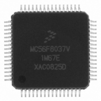
Manufacturer Part Number
MC56F8037VLH
Description
IC DSP 16BIT DUAL 64-LQFP
Manufacturer
Freescale Semiconductor
Series
56F8xxxr
Datasheet
1.MC56F8037EVM.pdf
(180 pages)
Specifications of MC56F8037VLH
Core Processor
56800
Core Size
16-Bit
Speed
32MHz
Connectivity
CAN, I²C, SCI, SPI
Peripherals
POR, PWM, WDT
Number Of I /o
53
Program Memory Size
64KB (32K x 16)
Program Memory Type
FLASH
Ram Size
4K x 16
Voltage - Supply (vcc/vdd)
3 V ~ 3.6 V
Data Converters
A/D 16x12b; D/A 2x12b
Oscillator Type
Internal
Operating Temperature
-40°C ~ 105°C
Package / Case
64-LQFP
Data Bus Width
16 bit
Processor Series
MC56F80xx
Core
56800E
Numeric And Arithmetic Format
Fixed-Point
Device Million Instructions Per Second
32 MIPs
Maximum Clock Frequency
32 MHz
Number Of Programmable I/os
53
Data Ram Size
8 KB
Operating Supply Voltage
3.3 V
Maximum Operating Temperature
+ 105 C
Mounting Style
SMD/SMT
Development Tools By Supplier
MC56F8037EVM
Interface Type
SCI, SPI, I2C
Minimum Operating Temperature
- 40 C
Package
64LQFP
Family Name
56F8xxx
Maximum Speed
32 MHz
On-chip Adc
2(8-chx10-bit)
On-chip Dac
2-chx12-bit
Number Of Timers
5
For Use With
MC56F8037EVM - BOARD EVAL FOR MC56F8037
Lead Free Status / RoHS Status
Lead free / RoHS Compliant
Eeprom Size
-
Lead Free Status / Rohs Status
Lead free / RoHS Compliant
Available stocks
Company
Part Number
Manufacturer
Quantity
Price

Company:
Part Number:
MC56F8037VLH
Manufacturer:
Freescale Semiconductor
Quantity:
10 000
Part Number:
MC56F8037VLH
Manufacturer:
NXP/恩智浦
Quantity:
20 000
Company:
Part Number:
MC56F8037VLHR
Manufacturer:
Freescale Semiconductor
Quantity:
10 000


6.3.23.5
This bit field is reserved. Each bit must be set to 0.
6.3.23.6
This field selects the alternate input source signal to feed Quad Timer A, input 1.
6.3.23.7
This bit field is reserved. Each bit must be set to 0.
For Timer A to detect the PWM SYNC signal, the clock rate of both the PWM module and Timer A
module must be identical, at either the system clock rate or 3X system clock rate.
6.4 Clock Generation Overview
The SIM uses the master clock (2X system clock) at a maximum of 64MHz from the OCCS module to
produce a system clock at a maximum of 32MHz for the peripheral, core and memory. It divides the master
clock by two and gates it with appropriate power mode and clock gating controls. A 3X system high-speed
peripheral clock input from OCCS operates at three times the system clock at a maximum of 96MHz and
can be an optional clock for PWM, Timer A, Timer B, and I
gating the 3X system high-speed peripheral clock with appropriate power mode and clock gating controls.
The OCCS configuration controls the operating frequency of the SIM’s master clocks. In the OCCS, either
an external clock (CLKIN), a crystal oscillator, or the relaxation oscillator can be selected as the master
clock source (MSTR_OSC). An external clock can be operated at any frequency up to 64MHz. The crystal
oscillator can be operated only at a maximum of 8MHz. The relaxation oscillator can be operated at full
speed (8MHz), standby speed (200kHz using ROSB), or powered down (using ROPD). An 8MHz
MSTR_OSC can be multiplied to 196MHz using the PLL and postscaled to provide a variety of high-speed
clock rates. Either the postscaled PLL output or MSTR_OSC signal can be selected to produce the master
clocks to the SIM. When the PLL is selected, both the 3X system clock and the 2X system clock are
enabled. If the PLL is not selected, the 3X system clock is disabled and the master clock is MSTR_OSC.
In combination with the OCCS module, the SIM provides power modes (see
and clock rate controls to provide flexible control of clocking and power utilization. The clock rate
controls enable the high-speed clocking option for the two quad timers (TMRA and TMRB) and PWM,
but requires the PLL to be on and selected. Refer to the 56F802x and 56F803x Peripheral Reference
Manual for further details. The peripheral clock enable controls can be used to disable an individual
peripheral clock when it is not used.
6.5 Power-Saving Modes
The 56F8037/56F8027 operates in one of five Power-Saving modes, as shown in
124
•
•
0 = I/O pin (External) - Use Timer A1 input/output pin
1 = CMPAO (Internal) - Use Comparator A output
Reserved—Bits 7–5
Select Peripheral Input Source for TA1 (IPS2_TA1)—Bit 4
Reserved—Bits 3–0
56F8037/56F8027 Data Sheet, Rev. 7
2
C modules. These clocks are generated by
Section
Table 6-2
Freescale Semiconductor
6.5), clock enables,
.
Related parts for MC56F8037VLH
Image
Part Number
Description
Manufacturer
Datasheet
Request
R

Part Number:
Description:
Manufacturer:
Freescale Semiconductor, Inc
Datasheet:
Part Number:
Description:
Manufacturer:
Freescale Semiconductor, Inc
Datasheet:
Part Number:
Description:
Manufacturer:
Freescale Semiconductor, Inc
Datasheet:
Part Number:
Description:
Manufacturer:
Freescale Semiconductor, Inc
Datasheet:
Part Number:
Description:
Manufacturer:
Freescale Semiconductor, Inc
Datasheet:
Part Number:
Description:
Manufacturer:
Freescale Semiconductor, Inc
Datasheet:
Part Number:
Description:
Manufacturer:
Freescale Semiconductor, Inc
Datasheet:
Part Number:
Description:
Manufacturer:
Freescale Semiconductor, Inc
Datasheet:
Part Number:
Description:
Manufacturer:
Freescale Semiconductor, Inc
Datasheet:
Part Number:
Description:
Manufacturer:
Freescale Semiconductor, Inc
Datasheet:
Part Number:
Description:
Manufacturer:
Freescale Semiconductor, Inc
Datasheet:
Part Number:
Description:
Manufacturer:
Freescale Semiconductor, Inc
Datasheet:
Part Number:
Description:
Manufacturer:
Freescale Semiconductor, Inc
Datasheet:
Part Number:
Description:
Manufacturer:
Freescale Semiconductor, Inc
Datasheet:
Part Number:
Description:
Manufacturer:
Freescale Semiconductor, Inc
Datasheet: