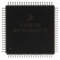
MCF52232CAF50 Freescale Semiconductor, MCF52232CAF50 Datasheet - Page 21

MCF52232CAF50
Manufacturer Part Number
MCF52232CAF50
Description
IC MCU 32BIT 128K FLASH 80-LQFP
Manufacturer
Freescale Semiconductor
Series
MCF5223xr
Datasheet
1.MCF52236AF50.pdf
(55 pages)
Specifications of MCF52232CAF50
Core Processor
Coldfire V2
Core Size
32-Bit
Speed
50MHz
Connectivity
Ethernet, I²C, SPI, UART/USART
Peripherals
DMA, LVD, POR, PWM, WDT
Number Of I /o
56
Program Memory Size
128KB (128K x 8)
Program Memory Type
FLASH
Ram Size
32K x 8
Voltage - Supply (vcc/vdd)
3 V ~ 3.6 V
Data Converters
A/D 8x12b
Oscillator Type
Internal
Operating Temperature
-40°C ~ 85°C
Package / Case
80-LQFP
Cpu Family
MCF5223x
Device Core
ColdFire
Device Core Size
32b
Frequency (max)
50MHz
Interface Type
I2C/QSPI/UART
Total Internal Ram Size
32KB
# I/os (max)
56
Number Of Timers - General Purpose
10
Operating Supply Voltage (typ)
3.3V
Operating Supply Voltage (max)
3.6V
Operating Supply Voltage (min)
3V
On-chip Adc
8-chx12-bit
Instruction Set Architecture
RISC
Operating Temp Range
-40C to 85C
Operating Temperature Classification
Industrial
Mounting
Surface Mount
Pin Count
80
Package Type
LQFP
Processor Series
MCF522x
Core
ColdFire V2
Data Bus Width
32 bit
Data Ram Size
32 KB
Maximum Clock Frequency
50 MHz
Number Of Programmable I/os
56
Number Of Timers
10
Maximum Operating Temperature
+ 85 C
Mounting Style
SMD/SMT
3rd Party Development Tools
JLINK-CF-BDM26, EWCF
Development Tools By Supplier
M52235EVB, M52233DEMO
Minimum Operating Temperature
- 40 C
Lead Free Status / RoHS Status
Lead free / RoHS Compliant
Eeprom Size
-
Lead Free Status / Rohs Status
Compliant
Available stocks
Company
Part Number
Manufacturer
Quantity
Price
Company:
Part Number:
MCF52232CAF50
Manufacturer:
FREESCAL
Quantity:
410
Company:
Part Number:
MCF52232CAF50
Manufacturer:
Freescale
Quantity:
221
Company:
Part Number:
MCF52232CAF50
Manufacturer:
Freescale Semiconductor
Quantity:
10 000
1
2
3
4
5
6
7
8
9
10
11
Pin Group
FlexCAN
UART 1
VDD
UART 2
The PDSR and PSSR registers are described in
All signals have a pull-up in GPIO mode.
The use of an external PHY limits ADC, interrupt, and QSPI functionality. It also disables the UART0/1 and timer pins.
The multiplexed CANTX and CANRX signals do not have dedicated pins, but are available as muxed replacements for other signals.
The VDD1, VDD2, VDDPLL, and PHY_VDD pins are for decoupling only and should not have power directly applied to them.
For primary and GPIO functions only.
Only when JTAG mode is enabled.
For secondary and GPIO functions only.
RSTI has an internal pull-up resistor; however, the use of an external resistor is strongly recommended.
For GPIO function. Primary Function has pull-up control within the GPT module.
This list for power and ground does not include those dedicated power/ground pins included elsewhere, e.g. in the Ethernet PHY.
(single-chip) mode.
VDDX
VSSX
VSS
5,11
3
Function
Primary
URXD1
URXD2
SYNCA
SYNCB
UCTS1
URTS1
UTXD1
UCTS2
URTS2
UTXD2
VDDX
VSSX
VDD
VSS
SecondaryF
CANTX
CANRX
unction
SYNCA
SYNCB
—
—
—
—
—
—
—
—
—
—
Table 3. Pin Functions by Primary and Alternate Purpose (continued)
4
4
FEC_TXD[0]
FEC_MDIO
FEC_MDC
FEC_COL
Function
Tertiary
URXD2
UTXD2
—
—
—
—
—
—
—
—
Chapter 14, “General Purpose I/O
Quaternary
Function
PUB[3]
PUB[2]
PUB[1]
PUB[0]
PUC[3]
PUC[2]
PUC[1]
PUC[0]
PAS[3]
PAS[2]
—
—
—
—
PDSR[14]
PDSR[12]
PDSR[27]
PDSR[26]
PDSR[25]
PDSR[39]
PDSR[39]
Strength/
PDSR[15]
PDSR[13]
PDSR[24]
Control
Drive
N/A
N/A
N/A
N/A
1
Module. All programmable signals default to 2mA drive in normal
Wired OR
PWOR[2]
PWOR[3]
Control
N/A
N/A
N/A
N/A
—
—
—
—
—
—
—
—
Pull-down
Pull-up/
—
—
—
—
—
—
—
—
—
—
—
—
—
—
2
D5, D6, E6, G5,
E4, E5, E7,F4,
F5, F6, F7, F8
G6, G7, H6
Pin on 121
MAPBGA
D7, E8
K10
K11
L10
L11
H3
K3
J3
L3
—
—
—
Pin on 112
65,102
64,101
14, 43
15, 42
LQFP
24
23
32
33
61
60
62
63
28
27
Pin on 80
LQFP
10, 31
11, 30
45,74
44,73
16
15
23
24
20
19
—
—
—
—


