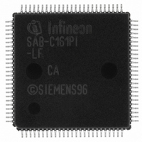
SAB-C161PI-LF CA Infineon Technologies, SAB-C161PI-LF CA Datasheet - Page 53

SAB-C161PI-LF CA
Manufacturer Part Number
SAB-C161PI-LF CA
Description
IC MICROCONTROLLER 16BIT 100TQFP
Manufacturer
Infineon Technologies
Series
C16xxr
Datasheet
1.SAF-C161PI-LM_CA.pdf
(82 pages)
Specifications of SAB-C161PI-LF CA
Core Processor
C166
Core Size
16-Bit
Speed
20MHz
Connectivity
EBI/EMI, I²C, SPI, UART/USART
Peripherals
POR, PWM, WDT
Number Of I /o
76
Program Memory Type
ROMless
Ram Size
3K x 8
Voltage - Supply (vcc/vdd)
4.5 V ~ 5.5 V
Data Converters
A/D 4x10b
Oscillator Type
Internal
Operating Temperature
0°C ~ 70°C
Package / Case
100-LFQFP
Packages
PG-TQFP-100
Max Clock Frequency
20.0 MHz
Sram (incl. Cache)
3.0 KByte
A / D Input Lines (incl. Fadc)
4
Program Memory
0.0 KByte
Lead Free Status / RoHS Status
Lead free / RoHS Compliant
Eeprom Size
-
Program Memory Size
-
Other names
B161PILFCAXT
SAB-C161PI-LF CA
SAB-C161PI-LFCAINTR
SABC161PILFCAXT
SP000014344
SAB-C161PI-LF CA
SAB-C161PI-LFCAINTR
SABC161PILFCAXT
SP000014344
A/D Converter Characteristics
(Operating Conditions apply)
4.0V (2.6V)
Parameter
Analog input voltage range
Basic clock frequency
Conversion time
Total unadjusted error
Internal resistance of
reference voltage source
Internal resistance of analog
source
ADC input capacitance
1)
2) The limit values for
3) This parameter includes the sample time
4) TUE is tested at
5) This case is not applicable for the reduced supply voltage range.
6) During the conversion the ADC’s capacitance must be repeatedly charged or discharged. The internal
7) Not 100% tested, guaranteed by design.
8) During the sample time the input capacitance
Data Sheet
SS
cases will be X000
result register with the conversion result.
Values for the basic clock
This parameter depends on the ADC control logic. It is not a real maximum value, but rather a fixum.
voltages within the defined voltage range.
The specified TUE is guaranteed only if an overload condition (see
selected analog input pins and the absolute sum of input overload currents on all analog input pins does not
exceed 10 mA.
During the reset calibration sequence the maximum TUE may be 4 LSB ( 8 LSB @ 3V).
resistance of the reference voltage source must allow the capacitance to reach its respective voltage level
within each conversion step. The maximum internal resistance results from the programmed conversion timing.
internal resistance of the analog source must allow the capacitance to reach its final voltage level within
After the end of the sample time
Values for the sample time
AIN
- 0.1V
may exceed
AGND
AREF
H
AGND
AREF
BC
or X3FF
must not be exceeded when selecting the CPU frequency and the ADCTC setting.
=5.0V (3.3V),
or
SS
DD
BC
AREF
S
H
+ 0.2V
, respectively.
depend on the conversion time programming.
depend on programming and can be taken from the table below.
+ 0.1V (Note the influence on TUE.)
S
up to the absolute maximum ratings. However, the conversion result in these
, changes of the analog input voltage have no effect on the conversion result.
Symbol
4)
TUE CC
BC
C
AIN
AREF
ASRC
AIN
AGND
S
, the time for determining the digital result and the time to load the
CC –
CC –
SR
SR –
SR –
=0V,
I
can be charged/discharged by the external source. The
0.5
–
–
DD
51
AGND
=4.9V (3.2V). It is guaranteed by design for all other
min.
Limit Values
6.25
40
- 0.25
- 0.25
33
S
BC
S
AREF
OV
+2
2
4
max.
/ 450
/ 60
specification) occurs on maximum 2 not
BC
CPU
+
Unit Test Condition
V
MHz
LSB
LSB
k
k
pF
1)
2)
3)
7)
CPU
BC
S
AREF
AREF
in [ns]
in [ns]
= 1 /
4.0 V
2.6 V
&3,
7) 8)
1999-07
6) 7)
CPU
5)
S
.


