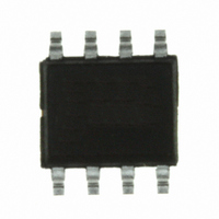
MC9S08QA4CDNE Freescale Semiconductor, MC9S08QA4CDNE Datasheet - Page 13

MC9S08QA4CDNE
Manufacturer Part Number
MC9S08QA4CDNE
Description
IC MCU 8BIT 4K FLASH 8-SOIC
Manufacturer
Freescale Semiconductor
Series
HCS08r
Datasheet
1.MC9S08QA2CFQE.pdf
(32 pages)
Specifications of MC9S08QA4CDNE
Core Processor
HCS08
Core Size
8-Bit
Speed
20MHz
Peripherals
LVD, POR, PWM, WDT
Number Of I /o
4
Program Memory Size
4KB (4K x 8)
Program Memory Type
FLASH
Ram Size
256 x 8
Voltage - Supply (vcc/vdd)
1.8 V ~ 3.6 V
Data Converters
A/D 4x10b
Oscillator Type
Internal
Operating Temperature
-40°C ~ 85°C
Package / Case
8-SOIC (3.9mm Width)
Processor Series
S08QA
Core
HCS08
Data Bus Width
8 bit
Data Ram Size
256 B
Interface Type
I2C, SCI, SPI
Maximum Clock Frequency
20 MHz
Number Of Programmable I/os
4
Number Of Timers
1
Operating Supply Voltage
3.6 V
Maximum Operating Temperature
+ 85 C
Mounting Style
SMD/SMT
3rd Party Development Tools
EWS08
Development Tools By Supplier
DEMO9S08QA4
Minimum Operating Temperature
- 40 C
On-chip Adc
4-ch x 10-bit
Lead Free Status / RoHS Status
Lead free / RoHS Compliant
Eeprom Size
-
Connectivity
-
Lead Free Status / Rohs Status
Lead free / RoHS Compliant
3.8.1
1
2
3
4
5
Freescale Semiconductor
Bus frequency (t
Real-time interrupt internal oscillator period (see
External reset pulse width
IRQ pulse width
KBIPx pulse width
Port rise and fall time (load = 50 pF)
BKGD/MS setup time after issuing background debug force
reset to enter user or BDM modes
BKGD/MS hold time after issuing background debug force
reset to enter user or BDM modes
Data in Typical column was characterized at 3.0 V, 25°C.
This is the shortest pulse that is guaranteed to be recognized.
This is the minimum pulse width that is guaranteed to pass through the pin synchronization circuitry. Shorter pulses may or
may not be recognized. In stop mode, the synchronizer is bypassed so shorter pulses can be recognized in that case.
Timing is shown with respect to 20% V
To enter BDM mode following a POR, BKGD/MS should be held low during the power-up and for a hold time of t
rises above V
Period (μs)
Control Timing
LVD
cyc
.
1600
1400
1200
1000
= 1/f
800
600
400
200
Slew rate control disabled (PTxSE = 0)
Slew rate control enabled (PTxSE = 1)
0
–40
Bus
Parameter
2
)
Figure 9. Typical RTI Clock Period vs. Temperature
–40
5
4
MC9S08QA4 Series MCU Data Sheet, Rev. 3
DD
Asynchronous path
Asynchronous path
Synchronous path
Synchronous path
and 80% V
0
Table 9. Control Timing
Table
Temperature (°C)
DD
20
9)
levels. Temperature range –40°C to 85°C.
2
3
2
3
t
t
40
Symbol
ILIH,
Rise
t
t
MSSU
t
t
f
extrst
t
MSH
ILIH
Bus
RTI
, t
t
IHIL
Fall
60
1.5 t
1.5 t
Min
700
100
100
100
500
100
—
—
0
cyc
cyc
80
Typical
100
1000
30
—
—
—
—
—
—
3
Electrical Characteristics
1
= +3 σ
= Mean
= –3 σ
1300
Max
10
—
—
—
—
—
—
—
MSH
after V
MHz
Unit
μs
ns
ns
ns
ns
ns
μs
DD
13


