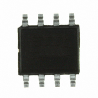
MC9S08QA4CDNE Freescale Semiconductor, MC9S08QA4CDNE Datasheet - Page 8

MC9S08QA4CDNE
Manufacturer Part Number
MC9S08QA4CDNE
Description
IC MCU 8BIT 4K FLASH 8-SOIC
Manufacturer
Freescale Semiconductor
Series
HCS08r
Datasheet
1.MC9S08QA2CFQE.pdf
(32 pages)
Specifications of MC9S08QA4CDNE
Core Processor
HCS08
Core Size
8-Bit
Speed
20MHz
Peripherals
LVD, POR, PWM, WDT
Number Of I /o
4
Program Memory Size
4KB (4K x 8)
Program Memory Type
FLASH
Ram Size
256 x 8
Voltage - Supply (vcc/vdd)
1.8 V ~ 3.6 V
Data Converters
A/D 4x10b
Oscillator Type
Internal
Operating Temperature
-40°C ~ 85°C
Package / Case
8-SOIC (3.9mm Width)
Processor Series
S08QA
Core
HCS08
Data Bus Width
8 bit
Data Ram Size
256 B
Interface Type
I2C, SCI, SPI
Maximum Clock Frequency
20 MHz
Number Of Programmable I/os
4
Number Of Timers
1
Operating Supply Voltage
3.6 V
Maximum Operating Temperature
+ 85 C
Mounting Style
SMD/SMT
3rd Party Development Tools
EWS08
Development Tools By Supplier
DEMO9S08QA4
Minimum Operating Temperature
- 40 C
On-chip Adc
4-ch x 10-bit
Lead Free Status / RoHS Status
Lead free / RoHS Compliant
Eeprom Size
-
Connectivity
-
Lead Free Status / Rohs Status
Lead free / RoHS Compliant
1
2
3
4
5
Electrical Characteristics
8
Power on reset (POR) re-arm voltage
Bandgap voltage reference
Input high voltage (V
Input high voltage (1.8 V ≤ V
Input low voltage (V
Input low voltage (1.8 V ≤ V
Input hysteresis (all digital inputs)
Input leakage current (per pin)
High impedance (off-state) leakage current (per pin)
Internal pullup resistors
Internal pulldown resistor (KBI)
Output high voltage — low drive (PTxDSn = 0)
Output high voltage — high drive (PTxDSn = 1)
Maximum total I
Output low voltage — low drive (PTxDSn = 0)
Output low voltage — high drive (PTxDSn = 1)
Maximum total I
DC injection current
Input capacitance (all non-supply pins)
RAM will retain data down to POR voltage. RAM data not guaranteed to be valid following a POR.
This parameter is characterized and not tested on each device.
Measurement condition for pull resistors: V
PTA5/IRQ/TCLK/RESET pullup resistor may not pull up to the specified minimum V
to guarantee that a logic 1 will be read on any port input when the pullup is enabled and no DC load is present on the pin.
All functional non-supply pins are internally clamped to V
I
I
I
I
I
I
Single pin limit
Total MCU limit, includes sum of all stressed pins
I
OH
OH
OH
OL
OL
OL
V
V
I
OL
OH
In
In
V
= 2.0 mA (V
= 6 mA (V
= 3 mA (V
= 10.0 mA (V
= –10 mA (V
= –6 mA (V
= –3 mA (V
= V
= V
= –2 mA (V
In
< V
DD
DD
Table 6. DC Characteristics (Temperature Range = –40 to 85°C Ambient) (continued)
SS
or V
or V
, V
OH
OL
DD
DD
SS
SS
DD
DD
DD
In
DD
for all port pins
DD
for all port pins
≥ 2.3 V)
≥ 1.8 V)
DD
DD
, all input/output
, all input-only pins
> V
DD
2, 5, 6, 7
≥ 2.3 V)
≥ 1.8 V)
≥ 1.8 V)
≥ 1.8 V)
≥ 2.7 V)
≥ 2.7 V)
> 2.3 V) (all digital inputs)
3,4
DD
> 2.3 V) (all digital inputs)
Parameter
DD
DD
≤ 2.3 V) (all digital inputs)
≤ 2.3 V) (all digital inputs)
MC9S08QA4 Series MCU Data Sheet, Rev. 3
In
= V
(V
SS
DD
for pullup and V
rising)
SS
and V
Symbol
|I
V
|I
V
V
R
R
V
DD
V
I
V
|I
OHT
C
V
OLT
I
OZ
hys
OH
por
BG
OL
IC
In
PU
PD
In
IH
IL
In
.
|
|
= V
|
DD
0.85 × V
0.70 × V
0.06 × V
for pulldown.
V
V
DD
DD
2.16
1.18
17.5
17.5
–0.2
Min
–5
—
—
—
—
—
—
—
—
—
—
—
—
– 0.5
– 0.5
IH
. However, all ports are functionally tested
DD
DD
DD
Typical
0.025
0.025
2.19
1.20
1.4
—
—
—
—
—
—
—
—
—
—
—
—
—
—
—
—
—
—
—
—
Freescale Semiconductor
0.35 × V
0.30 × V
Max
2.27
1.21
52.5
52.5
1.0
1.0
0.5
0.5
0.5
0.5
0.2
60
60
—
—
—
—
—
—
—
—
5
7
DD
DD
Unit
mA
mA
mA
mA
μA
μA
kΩ
kΩ
pF
V
V
V
V
V
V
V


