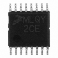
MCL908QY2CDTE Freescale Semiconductor, MCL908QY2CDTE Datasheet - Page 45

MCL908QY2CDTE
Manufacturer Part Number
MCL908QY2CDTE
Description
IC MCU 8BIT 1.5K FLASH 16-TSSOP
Manufacturer
Freescale Semiconductor
Series
HC08r
Datasheet
1.MCL908QY2CDWE.pdf
(182 pages)
Specifications of MCL908QY2CDTE
Core Processor
HC08
Core Size
8-Bit
Speed
2MHz
Peripherals
LVD, POR, PWM
Number Of I /o
13
Program Memory Size
1.5KB (1.5K x 8)
Program Memory Type
FLASH
Ram Size
128 x 8
Voltage - Supply (vcc/vdd)
2.4 V ~ 3.6 V
Data Converters
A/D 4x8b
Oscillator Type
Internal
Operating Temperature
-40°C ~ 85°C
Package / Case
16-TSSOP
Lead Free Status / RoHS Status
Lead free / RoHS Compliant
Eeprom Size
-
Connectivity
-
- Current page: 45 of 182
- Download datasheet (2Mb)
3.7.3 ADC Input Clock Register
This register selects the clock frequency for the ADC.
ADIV2–ADIV0 — ADC Clock Prescaler Bits
Freescale Semiconductor
ADIV2, ADIV1, and ADIV0 form a 3-bit field which selects the divide ratio used by the ADC to generate
the internal ADC clock.
set according to the MCU operating voltage. Lower operating voltages will require lower ADC clock
frequencies for best accuracy. The analog input level should remain stable for the entire conversion
time (maximum = 17 ADC clock cycles).
Address: $003F
Reset:
Read:
Write:
ADIV2
Bit 7
0
X = don’t care
ADIV2
Table 3-2
Figure 3-5. ADC Input Clock Register (ADICLK)
0
0
0
0
1
= Unimplemented
MC68HLC908QY/QT Family Data Sheet, Rev. 3
ADIV1
6
0
Table 3-2. ADC Clock Divide Ratio
shows the available clock configurations. The ADC clock should be
ADIV1
X
0
0
1
1
ADIV0
5
0
ADIV0
X
0
1
0
1
4
0
0
3
0
0
ADC Clock Rate
Bus clock ÷ 16
Bus clock ÷ 1
Bus clock ÷ 2
Bus clock ÷ 4
Bus clock ÷ 8
2
0
0
1
0
0
Input/Output Registers
Bit 0
0
0
45
Related parts for MCL908QY2CDTE
Image
Part Number
Description
Manufacturer
Datasheet
Request
R
Part Number:
Description:
Manufacturer:
Freescale Semiconductor, Inc
Datasheet:
Part Number:
Description:
Manufacturer:
Freescale Semiconductor, Inc
Datasheet:
Part Number:
Description:
Manufacturer:
Freescale Semiconductor, Inc
Datasheet:
Part Number:
Description:
Manufacturer:
Freescale Semiconductor, Inc
Datasheet:
Part Number:
Description:
Manufacturer:
Freescale Semiconductor, Inc
Datasheet:
Part Number:
Description:
Manufacturer:
Freescale Semiconductor, Inc
Datasheet:
Part Number:
Description:
Manufacturer:
Freescale Semiconductor, Inc
Datasheet:
Part Number:
Description:
Manufacturer:
Freescale Semiconductor, Inc
Datasheet:
Part Number:
Description:
Manufacturer:
Freescale Semiconductor, Inc
Datasheet:
Part Number:
Description:
Manufacturer:
Freescale Semiconductor, Inc
Datasheet:
Part Number:
Description:
Manufacturer:
Freescale Semiconductor, Inc
Datasheet:
Part Number:
Description:
Manufacturer:
Freescale Semiconductor, Inc
Datasheet:
Part Number:
Description:
Manufacturer:
Freescale Semiconductor, Inc
Datasheet:
Part Number:
Description:
Manufacturer:
Freescale Semiconductor, Inc
Datasheet:
Part Number:
Description:
Manufacturer:
Freescale Semiconductor, Inc
Datasheet:


