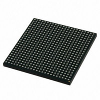
MCIMX512CJM6C Freescale Semiconductor, MCIMX512CJM6C Datasheet - Page 131

MCIMX512CJM6C
Manufacturer Part Number
MCIMX512CJM6C
Description
MULTIMEDIA PROC 529-LFBGA
Manufacturer
Freescale Semiconductor
Series
i.MX51r
Specifications of MCIMX512CJM6C
Core Processor
ARM Cortex-A8
Core Size
32-Bit
Speed
600MHz
Connectivity
1-Wire, EBI/EMI, Ethernet, I²C, IrDA, MMC, SPI, SSI, UART/USART, USB OTG
Peripherals
DMA, I²S, LCD, POR, PWM, WDT
Number Of I /o
128
Program Memory Type
ROMless
Ram Size
128K x 8
Voltage - Supply (vcc/vdd)
0.8 V ~ 1.15 V
Oscillator Type
External
Operating Temperature
-20°C ~ 85°C
Package / Case
529-LFBGA
Operating Temperature (min)
-40C
Operating Temperature Classification
Industrial
Mounting
Surface Mount
Processor Series
i.MX51
Core
ARM Cortex A8
Data Bus Width
32 bit
Program Memory Size
36 KB
Data Ram Size
128 KB
Interface Type
I2C, SPI, SSI, UART, USB
Maximum Clock Frequency
200 MHz
Number Of Timers
5
Operating Supply Voltage
0.8 V to 1.15 V
Maximum Operating Temperature
+ 95 C
Mounting Style
SMD/SMT
3rd Party Development Tools
MDK-ARM, RL-ARM, ULINK2
Development Tools By Supplier
MCIMX51EVKJ
Minimum Operating Temperature
- 40 C
Lead Free Status / RoHS Status
Lead free / RoHS Compliant
Eeprom Size
-
Program Memory Size
-
Data Converters
-
Lead Free Status / Rohs Status
Compliant
- Current page: 131 of 200
- Download datasheet (6Mb)
4.7.15.1 SSI Transmitter Timing with Internal Clock
Figure 91
the SSI transmitter internal clock.
Freescale Semiconductor
.
AUDMUX port 6
AUDMUX port 7
depicts the SSI transmitter internal clock timing and
Note: SRXD input in synchronous mode only
TXFS (wl)
(Output)
TXFS (bl)
(Output)
•
•
Port
RXD
(Input)
TXC
(Output)
TXD
(Output)
i.MX51 Applications Processors for Consumer and Industrial Products, Rev. 4
The terms WL and BL used in the timing diagrams and tables refer to
Word Length (WL) and Bit Length (BL).
The SSI timing diagrams use generic signal names wherein the names
used in the i.MX51 Multimedia Applications Processor Reference
Manual (MCIMX51RM) are channel specific signal names. For
example, a channel clock referenced in the IOMUXC chapter as
AUD3_TXC appears in the timing diagram as TXC.
Figure 91. SSI Transmitter Internal Clock Timing Diagram
SS2
Table 101. AUDMUX Port Allocation (continued)
SS6
Signal Nomenclature
SS1
AUD6
SSI 3
SS10
SS16
SS8
NOTE
SS42
SS43
SS5
SS4
External—EIM or DISP2 via IOMUX
Internal
SS14
Table 102
SS17
Type and Access
lists the timing parameters for
SS3
SS15
SS19
SS18
Electrical Characteristics
SS12
131
Related parts for MCIMX512CJM6C
Image
Part Number
Description
Manufacturer
Datasheet
Request
R
Part Number:
Description:
MCIMX-LVDS1
Manufacturer:
Freescale Semiconductor
Datasheet:
Part Number:
Description:
Manufacturer:
Freescale Semiconductor, Inc
Datasheet:
Part Number:
Description:
Manufacturer:
Freescale Semiconductor, Inc
Datasheet:
Part Number:
Description:
Manufacturer:
Freescale Semiconductor, Inc
Datasheet:
Part Number:
Description:
Manufacturer:
Freescale Semiconductor, Inc
Datasheet:
Part Number:
Description:
Manufacturer:
Freescale Semiconductor, Inc
Datasheet:
Part Number:
Description:
Manufacturer:
Freescale Semiconductor, Inc
Datasheet:
Part Number:
Description:
Manufacturer:
Freescale Semiconductor, Inc
Datasheet:
Part Number:
Description:
Manufacturer:
Freescale Semiconductor, Inc
Datasheet:
Part Number:
Description:
Manufacturer:
Freescale Semiconductor, Inc
Datasheet:
Part Number:
Description:
Manufacturer:
Freescale Semiconductor, Inc
Datasheet:
Part Number:
Description:
Manufacturer:
Freescale Semiconductor, Inc
Datasheet:
Part Number:
Description:
Manufacturer:
Freescale Semiconductor, Inc
Datasheet:
Part Number:
Description:
Manufacturer:
Freescale Semiconductor, Inc
Datasheet:
Part Number:
Description:
Manufacturer:
Freescale Semiconductor, Inc
Datasheet:


