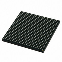
MCIMX512CJM6C Freescale Semiconductor, MCIMX512CJM6C Datasheet - Page 63

MCIMX512CJM6C
Manufacturer Part Number
MCIMX512CJM6C
Description
MULTIMEDIA PROC 529-LFBGA
Manufacturer
Freescale Semiconductor
Series
i.MX51r
Specifications of MCIMX512CJM6C
Core Processor
ARM Cortex-A8
Core Size
32-Bit
Speed
600MHz
Connectivity
1-Wire, EBI/EMI, Ethernet, I²C, IrDA, MMC, SPI, SSI, UART/USART, USB OTG
Peripherals
DMA, I²S, LCD, POR, PWM, WDT
Number Of I /o
128
Program Memory Type
ROMless
Ram Size
128K x 8
Voltage - Supply (vcc/vdd)
0.8 V ~ 1.15 V
Oscillator Type
External
Operating Temperature
-20°C ~ 85°C
Package / Case
529-LFBGA
Operating Temperature (min)
-40C
Operating Temperature Classification
Industrial
Mounting
Surface Mount
Processor Series
i.MX51
Core
ARM Cortex A8
Data Bus Width
32 bit
Program Memory Size
36 KB
Data Ram Size
128 KB
Interface Type
I2C, SPI, SSI, UART, USB
Maximum Clock Frequency
200 MHz
Number Of Timers
5
Operating Supply Voltage
0.8 V to 1.15 V
Maximum Operating Temperature
+ 95 C
Mounting Style
SMD/SMT
3rd Party Development Tools
MDK-ARM, RL-ARM, ULINK2
Development Tools By Supplier
MCIMX51EVKJ
Minimum Operating Temperature
- 40 C
Lead Free Status / RoHS Status
Lead free / RoHS Compliant
Eeprom Size
-
Program Memory Size
-
Data Converters
-
Lead Free Status / Rohs Status
Compliant
- Current page: 63 of 200
- Download datasheet (6Mb)
4.6.8
4.6.8.1
Figure 31
for this diagram is shown in
1
Freescale Semiconductor
This parameter is affected by pad timing. if the slew rate is < 1 V/ns, 0.2 ns should be added to the value. For cmos65 pads
this is true for medium and low drive strengths.
DD1
DD2
DD3
DD4
DD5
DD6
DD7
ID
SDCLK
SDCLK
ADDR
RAS
CAS
SDRAM clock high-level width
SDRAM clock low-level width
SDRAM clock cycle time
CS, RAS, CAS, CKE, WE setup time
CS, RAS, CAS, CKE, WE hold time
Address output setup time
Address output hold time
WE
shows the basic timing parameters for mobile DDR (mDDR) SDRAM. The timing parameters
CS
SDRAM Controller Timing Parameters
Mobile DDR SDRAM Timing Parameters
DD6
DD4
i.MX51 Applications Processors for Consumer and Industrial Products, Rev. 4
Parameter
ROW/BA
Figure 31. mDDR SDRAM Basic Timing Parameters
DD5
Table
Table 55. mDDR SDRAM Timing Parameter Table
DD5
DD7
55.
DD4
DD4
COL/BA
Symbol
t
t
t
t
t
t
t
IS
IH
IS
IH
CH
CK
CL
1
1
1
1
DD5
DD5
0.45
0.45
Min
0.9
0.9
0.9
0.9
5
200 MHz
DD1
DD3
Max
0.55
0.55
—
—
—
—
—
DD2
0.45
0.45
Min
1.1
1.1
1.1
1.1
6
166 MHz
Max
0.55
0.55
—
—
—
—
—
Electrical Characteristics
0.45
0.45
Min
7.5
1.3
1.3
1.3
1.3
133 MHz
Max
0.55
0.55
—
—
—
—
—
Unit
t
t
ns
ns
ns
ns
ns
CK
CK
63
Related parts for MCIMX512CJM6C
Image
Part Number
Description
Manufacturer
Datasheet
Request
R
Part Number:
Description:
MCIMX-LVDS1
Manufacturer:
Freescale Semiconductor
Datasheet:
Part Number:
Description:
Manufacturer:
Freescale Semiconductor, Inc
Datasheet:
Part Number:
Description:
Manufacturer:
Freescale Semiconductor, Inc
Datasheet:
Part Number:
Description:
Manufacturer:
Freescale Semiconductor, Inc
Datasheet:
Part Number:
Description:
Manufacturer:
Freescale Semiconductor, Inc
Datasheet:
Part Number:
Description:
Manufacturer:
Freescale Semiconductor, Inc
Datasheet:
Part Number:
Description:
Manufacturer:
Freescale Semiconductor, Inc
Datasheet:
Part Number:
Description:
Manufacturer:
Freescale Semiconductor, Inc
Datasheet:
Part Number:
Description:
Manufacturer:
Freescale Semiconductor, Inc
Datasheet:
Part Number:
Description:
Manufacturer:
Freescale Semiconductor, Inc
Datasheet:
Part Number:
Description:
Manufacturer:
Freescale Semiconductor, Inc
Datasheet:
Part Number:
Description:
Manufacturer:
Freescale Semiconductor, Inc
Datasheet:
Part Number:
Description:
Manufacturer:
Freescale Semiconductor, Inc
Datasheet:
Part Number:
Description:
Manufacturer:
Freescale Semiconductor, Inc
Datasheet:
Part Number:
Description:
Manufacturer:
Freescale Semiconductor, Inc
Datasheet:


