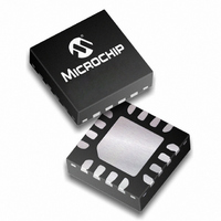
PIC16F688-E/ML Microchip Technology, PIC16F688-E/ML Datasheet - Page 102

PIC16F688-E/ML
Manufacturer Part Number
PIC16F688-E/ML
Description
IC PIC MCU FLASH 4KX14 16QFN
Manufacturer
Microchip Technology
Series
PIC® 16Fr
Datasheets
1.PIC16F616T-ISL.pdf
(8 pages)
2.PIC16F688T-ISL.pdf
(204 pages)
3.PIC16F688T-ISL.pdf
(6 pages)
4.PIC16F688T-ISL.pdf
(4 pages)
5.PIC16F688T-ISL.pdf
(688 pages)
Specifications of PIC16F688-E/ML
Core Size
8-Bit
Program Memory Size
7KB (4K x 14)
Core Processor
PIC
Speed
20MHz
Connectivity
UART/USART
Peripherals
Brown-out Detect/Reset, POR, WDT
Number Of I /o
12
Program Memory Type
FLASH
Eeprom Size
256 x 8
Ram Size
256 x 8
Voltage - Supply (vcc/vdd)
2 V ~ 5.5 V
Data Converters
A/D 8x10b
Oscillator Type
Internal
Operating Temperature
-40°C ~ 125°C
Package / Case
16-QFN
Controller Family/series
PIC16F
No. Of I/o's
12
Eeprom Memory Size
256Byte
Ram Memory Size
256Byte
Cpu Speed
20MHz
No. Of Timers
2
Processor Series
PIC16F
Core
PIC
Data Bus Width
8 bit
Data Ram Size
256 B
Interface Type
EUSART, RS- 232, SCI, USB
Maximum Clock Frequency
20 MHz
Number Of Programmable I/os
12
Number Of Timers
2
Maximum Operating Temperature
+ 125 C
Mounting Style
SMD/SMT
3rd Party Development Tools
52715-96, 52716-328, 52717-734
Development Tools By Supplier
PG164130, DV164035, DV244005, DV164005, PG164120, ICE2000, DM163014, DM164120-4
Minimum Operating Temperature
- 40 C
On-chip Adc
10 bit, 8 Channel
Lead Free Status / RoHS Status
Lead free / RoHS Compliant
For Use With
AC164324 - MODULE SKT FOR MPLAB 8DFN/16QFNXLT16QFN1 - SOCKET TRANSITION 14DIP TO 16QFNAC162061 - HEADER INTRFC MPLAB ICD2 20PINAC162056 - HEADER INTERFACE ICD2 16F688
Lead Free Status / Rohs Status
Details
- PIC16F616T-ISL PDF datasheet
- PIC16F688T-ISL PDF datasheet #2
- PIC16F688T-ISL PDF datasheet #3
- PIC16F688T-ISL PDF datasheet #4
- PIC16F688T-ISL PDF datasheet #5
- Current page: 102 of 688
- Download datasheet (3Mb)
PICmicro MID-RANGE MCU FAMILY
6.3
6.3.1
6.3.2
DS31006A-page 6-8
General Purpose Registers (GPR)
Special Function Registers (SFR)
Data Memory Organization
Data memory is made up of the Special Function Registers (SFR) area, and the General Pur-
pose Registers (GPR) area. The SFRs control the operation of the device, while GPRs are the
general area for data storage and scratch pad operations.
The data memory is banked for both the GPR and SFR areas. The GPR area is banked to allow
greater than 96 bytes of general purpose RAM to be addressed. SFRs are for the registers that
control the peripheral and core functions. Banking requires the use of control bits for bank selec-
tion. These control bits are located in the STATUS Register (STATUS<7:5>).
one of the data memory map organizations, this organization is device dependent.
To move values from one register to another register, the value must pass through the W register.
This means that for all register-to-register moves, two instruction cycles are required.
The entire data memory can be accessed either directly or indirectly. Direct addressing may
require the use of the RP1:RP0 bits. Indirect addressing requires the use of the File Select Reg-
ister (FSR). Indirect addressing uses the Indirect Register Pointer (IRP) bit of the STATUS regis-
ter for accesses into the Bank0 / Bank1 or the Bank2 / Bank3 areas of data memory.
Some Mid-Range MCU devices have banked memory in the GPR area. GPRs are not initialized
by a Power-on Reset and are unchanged on all other resets.
The register file can be accessed either directly, or using the File Select Register FSR, indirectly.
Some devices have areas that are shared across the data memory banks, so a read / write to
that area will appear as the same location (value) regardless of the current bank. We refer to this
area as the Common RAM.
The SFRs are used by the CPU and Peripheral Modules for controlling the desired operation of
the device. These registers are implemented as static RAM.
The SFRs can be classified into two sets, those associated with the “core” function and those
related to the peripheral functions. Those registers related to the “core” are described in this sec-
tion, while those related to the operation of the peripheral features are described in the section
of that peripheral feature.
All Mid-Range MCU devices have banked memory in the SFR area. Switching between these
banks requires the RP0 and RP1 bits in the STATUS register to be configured for the desired
bank. Some SFRs are initialized by a Power-on Reset and other resets, while other SFRs are
unaffected.
The register file can be accessed either directly, or using the File Select Register FSR, indirectly.
Note:
The Special Function Register (SFR) Area may have General Purpose Registers
(GPRs) mapped in these locations.
1997 Microchip Technology Inc.
Figure 6-5
shows
Related parts for PIC16F688-E/ML
Image
Part Number
Description
Manufacturer
Datasheet
Request
R

Part Number:
Description:
Manufacturer:
Microchip Technology Inc.
Datasheet:

Part Number:
Description:
IC PIC MCU FLASH 4KX14 14SOIC
Manufacturer:
Microchip Technology
Datasheet:

Part Number:
Description:
IC MCU FLASH 4KX14 14TSSOP
Manufacturer:
Microchip Technology
Datasheet:

Part Number:
Description:
IC PIC MCU FLASH 4KX14 14DIP
Manufacturer:
Microchip Technology
Datasheet:

Part Number:
Description:
IC PIC MCU FLASH 4KX14 16QFN
Manufacturer:
Microchip Technology
Datasheet:

Part Number:
Description:
IC MCU PIC FLASH 4KX14 14SOIC
Manufacturer:
Microchip Technology
Datasheet:

Part Number:
Description:
IC PIC MCU FLASH 4KX14 14TSSOP
Manufacturer:
Microchip Technology
Datasheet:

Part Number:
Description:
IC MCU PIC FLASH 4KX14 14DIP
Manufacturer:
Microchip Technology
Datasheet:

Part Number:
Description:
IC PIC MCU FLASH 4KX14 14TSSOP
Manufacturer:
Microchip Technology
Datasheet:

Part Number:
Description:
IC, 8BIT MCU, PIC16F, 32MHZ, SOIC-18
Manufacturer:
Microchip Technology
Datasheet:

Part Number:
Description:
IC, 8BIT MCU, PIC16F, 32MHZ, SSOP-20
Manufacturer:
Microchip Technology
Datasheet:

Part Number:
Description:
IC, 8BIT MCU, PIC16F, 32MHZ, DIP-18
Manufacturer:
Microchip Technology
Datasheet:

Part Number:
Description:
IC, 8BIT MCU, PIC16F, 32MHZ, QFN-28
Manufacturer:
Microchip Technology
Datasheet:

Part Number:
Description:
IC, 8BIT MCU, PIC16F, 32MHZ, QFN-28
Manufacturer:
Microchip Technology
Datasheet:

Part Number:
Description:
IC, 8BIT MCU, PIC16F, 32MHZ, QFN-28
Manufacturer:
Microchip Technology
Datasheet:


